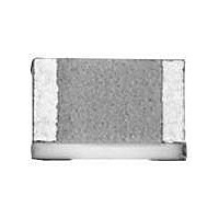
P1206Y1003BN Vishay, P1206Y1003BN Datasheet - Page 9

P1206Y1003BN
Manufacturer Part Number
P1206Y1003BN
Description
THIN FILM SFERNICE / P 1206 Y 1003 B N WP E2
Manufacturer
Vishay
Series
Pr
Datasheet
1.P1206E10R0BB.pdf
(10 pages)
Specifications of P1206Y1003BN
Resistance
100 KOhms
Tolerance
0.1 %
Package / Case
1206 (3216 metric)
Power Rating
0.33 Watt (1/3 Watt)
Voltage Rating
200 Volts
Operating Temperature Range
- 55 C to + 155 C
Termination Style
SMD/SMT
Dimensions
1.6 mm W x 3.06 mm L x 0.5 mm H
Product
Precision Resistors Thin Film SMD
Temperature Coefficient
+/- 10 PPM / C
Lead Free Status / RoHS Status
Lead free / RoHS Compliant
Lead Free Status / RoHS Status
Lead free / RoHS Compliant
P
Vishay Sfernice
Notes
• Chips ready to be trimmed available. (P
(1)
(2)
QUICK PROTOTYPING
Vishay Sfernice can offer quick prototyping service in 3 weeks production time for most popular case sizes: 0603, 0805, 1206
(Best tolerance: 0.05 %, best TCR: 10 ppm/°C) - Premium will apply - Check availability
www.vishay.com
68
HISTORICAL
GLOBAL PART NUMBER INFORMATION
New Global Part Numbering: P0505Y1003BBT0933
Historical Part Number example: P 0505 Y 1003 B B TR R0933 e2
For specific quantity of parts per packaging please consult Vishay Sfernice.
For paper tape please consult Vishay Sfernice.
MODEL
GLOBAL
MODEL
P
P
P
P
0
0505
SIZE
0302
0402
0505
0603
0705
0805
1005
1206
1505
2010
5
SIZE
0302
0402
0505
0603
0705
0805
1005
1206
1505
2010
K = ± 100 ppm/°C
H = ± 50 ppm/°C
E = ± 25 ppm/°C
Y = ± 10 ppm/°C
C = ± 5 ppm
Z = ± 5 ppm
X = Jumper
+ 155 °C)
(0.70 °C)
(- 55 °C;
High Precision Wraparound - Wide Ohmic Value Range
TCR
0
Y
H = ± 50 ppm/°C
E = ± 25 ppm/°C
Y = ± 10 ppm/°C
± 100 ppm/°C
C = ± 5 ppm
Z = ± 5 ppm
X = Jumper
5
+ 155 °C)
(0.70 °C)
(- 55 °C;
TCR
trim
K =
The first three digits
are significant figures
and
specifies the number
of zeros to follow, R
designates
point
10R0 = 10
3901 = 3900
1004 = 1 M
0R00 = Jumper
) - Please consult Vishay Sfernice.
For technical questions, contact:
Y
the
VALUE
Thin Film Chip Resistors
1003
1
The first three digits
are significant figures
and
specifies the number
of zeros to follow, R
designates
point
10R0 = 10
3901 = 3900
1004 = 1 M
0R00 = Jumper
last
decimal
the
digit
0
VALUE
last
TOLERANCE
W = ± 0.05 %
P = ± 0.02 %
C = ± 0.25 %
L = ± 0.01 %
decimal
B = ± 0.1 %
D = ± 0.5 %
0
X = Jumper
G = ± 2 %
F = ± 1 %
J = ± 5 %
digit
B
3
sfer@vishay.com
TOLERANCE
W = ± 0.05 %
L = ± 0.01 %
P = ± 0.02 %
C = ± 0.25 %
B = ± 0.1 %
D = ± 0.5 %
X = Jumper
G = ± 2 %
F = ± 1 %
J = ± 5 %
TERMINATION PACKAGING
B
B: SnPb over
N: SnAg over
nickel barrier
nickel barrier
G: Gold over
nickel barrier
N and G: Lead (Pb)-free/
B: Lead bearing version
B
RoHS version
B
TERMINATION PACKAGING
B: SnPb over
N: SnAg over
nickel barrier
nickel barrier
G: Gold over
nickel barrier
N and G: Lead (Pb)-free/
T
B: Lead bearing version
TR = Tape
Waffle pack
Blank =
RoHS version
TR
0
(1)
Document Number: 53017
Waffle pack
T = Tape
PT = Paper
Leave blank
9
if no option
Blank =
tape
OPTION
R0933
Revision: 14-Feb-11
(2)
3
(1)
blank if no
OPTION
Tin/silver
Leave
option
3
RoHS
blank:
SnPb
Gold
e2:
e4:
e2


