AD7298-1BCPZ Analog Devices Inc, AD7298-1BCPZ Datasheet - Page 21
AD7298-1BCPZ
Manufacturer Part Number
AD7298-1BCPZ
Description
8Channel 10Bit SAR
Manufacturer
Analog Devices Inc
Datasheet
1.AD7298-1BCPZ.pdf
(24 pages)
Specifications of AD7298-1BCPZ
Number Of Bits
10
Sampling Rate (per Second)
1M
Data Interface
Serial, SPI™
Number Of Converters
1
Power Dissipation (max)
23mW
Voltage Supply Source
Single Supply
Operating Temperature
-40°C ~ 125°C
Mounting Type
Surface Mount
Package / Case
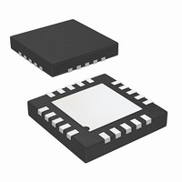
20-WFQFN, CSP Exposed Pad
Resolution (bits)
10bit
Sampling Rate
1MSPS
Input Channel Type
Single Ended
Supply Voltage Range - Analog
1.65V To 3.6V
Digital Ic Case Style
LFCSP
Rohs Compliant
Yes
Lead Free Status / RoHS Status
Lead free / RoHS Compliant
Available stocks
Company
Part Number
Manufacturer
Quantity
Price
Company:

Part Number:
AD7298-1BCPZ
Manufacturer:
ADI
Quantity:
200


LAYOUT AND CONFIGURATION
For optimum performance, carefully consider the power supply
and ground return layout on any PCB where the AD7298-1 is
used. The PCB containing the AD7298-1 should have separate
analog and digital sections, each having its own area of the board.
The AD7298-1 should be located in the analog section on any PCB.
Decouple the power supply to the AD7298-1 to ground with
10 µF and 0.1 µF capacitors. Place the capacitors as physically
close as possible to the device, with the 0.1 µF capacitor ideally
right up against the device. It is important that the 0.1 µF
capacitor has low effective series resistance (ESR) and low
effective series inductance (ESL); common ceramic types of
capacitors are suitable. The 0.1 µF capacitors provide a low
impedance path to ground for high frequencies caused by
transient currents due to internal logic switching. The 10 µF
capacitors are the tantalum bead type.
Rev. A | Page 21 of 24
The power supply line should have as large a trace as possible to
provide a low impedance path and reduce glitch effects on the
supply line. Shield clocks and other components with fast switching
digital signals from other parts of the board by a digital ground.
Avoid crossover of digital and analog signals, if possible. When
traces cross on opposite sides of the board, ensure that they run
at right angles to each other to reduce feedthrough effects on
the board.
The best board layout technique is the microstrip technique where
the component side of the board is dedicated to the ground
plane only, and the signal traces are placed on the solder side;
however, this is not always possible with a 2-layer board.
AD7298-1
Related parts for AD7298-1BCPZ
Image
Part Number
Description
Manufacturer
Datasheet
Request
R

Part Number:
Description:
±1.7g Dual-Axis IMEMS Accelerometer Evaluation Board
Manufacturer:
Analog Devices Inc
Datasheet:

Part Number:
Description:
Inertial Sensor Evaluation System
Manufacturer:
Analog Devices Inc
Datasheet:
Part Number:
Description:
Manufacturer:
Analog Devices Inc
Datasheet:
Part Number:
Description:
Manufacturer:
Analog Devices Inc
Datasheet:
Part Number:
Description:
Manufacturer:
Analog Devices Inc
Datasheet:
Part Number:
Description:
Manufacturer:
Analog Devices Inc
Datasheet:
Part Number:
Description:
Manufacturer:
Analog Devices Inc
Datasheet:
Part Number:
Description:
Manufacturer:
Analog Devices Inc
Datasheet:
Part Number:
Description:
Manufacturer:
Analog Devices Inc
Datasheet:
Part Number:
Description:
Manufacturer:
Analog Devices Inc
Datasheet:
Part Number:
Description:
Manufacturer:
Analog Devices Inc
Datasheet:
Part Number:
Description:
Manufacturer:
Analog Devices Inc
Datasheet: