AD260BND-0 Analog Devices Inc, AD260BND-0 Datasheet - Page 6
AD260BND-0
Manufacturer Part Number
AD260BND-0
Description
Power Supply IC
Manufacturer
Analog Devices Inc
Series
IsoLogic™r
Datasheet
1.AD260AND-0.pdf
(8 pages)
Specifications of AD260BND-0
Output Current Min
-25mA
Output Current Max
25mA
Rohs Status
RoHS non-compliant
Inputs - Side 1/side 2
0/5
Number Of Channels
5
Isolation Rating
3500Vrms
Voltage - Supply
4 V ~ 5.75 V
Data Rate
40MBd
Propagation Delay
14ns
Output Type
Tri-State
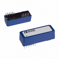
Package / Case
22-DIP Module
Operating Temperature
-25°C ~ 85°C
Lead Free Status / RoHS Status


AD260
(Continued from page 1)
Integral Isolated Power: The AD260 includes an integral,
uncommitted and flexible 1 Watt power transformer for devel-
oping isolated field power sources.
Field and System Enable Functions: Both the isolated and
nonisolated sides of the AD260 have ENABLE pins that three-
state all outputs. Upon reenabling these pins, all outputs are
updated to reflect the current input logic level.
CE Certifiable: Simply by adding the external bypass capacitors
at the supply pins, the AD260 can attain CE certification in
most applications (to the EMC directive) and conformance to
the low voltage (safety) directive is assured by the EN60950
certification.
GENERAL ATTRIBUTES
The AD260 provides five HCMOS/ACMOS compatible isolated
logic lines with
The case design and pin arrangement provides greater than
18 mm spacing between field and system side conductors, pro-
viding CSA/IS and IEC creepage spacing consistent with 750 V
mains isolation.
The five unidirectional logic lines have six possible combina-
tions of “ins” and “outs,” or transmitter/receiver pairs; hence
there are six AD260 part configurations (see Table I).
Each 20 MHz logic line has a Schmidt trigger input and a three-
state output (on the other side of the isolation barrier) and 14 ns of
propagation delay. A single enable pin on either side of the
barrier causes all outputs on that side to go three-state and all
inputs (driven pins) to ignore their inputs and retain their last
known state.
Note: All unused logic inputs (1–5) should be tied either high or low,
but not left floating.
10 kV/ s common-mode transient immunity.
INPUT
OUTPUT
63%
+3V
+2V
CAPACITANCE
TOTAL DELAY = (
INPUT
5pF
EFFECTIVE CIRCUIT MODEL FOR ONE ISOLATED LOGIC LINE
t
PD
t
Figure 2. Typical Timing and Delay Models
PLH
t
t
rr
PLH
=
SCHMITT
TRIGGER
t
OR
ff
= 100
t
PHL
= 5.5ns INTO 50pF
0.5ns – NO LOAD
) =
PROPAGATION DELAY
x C
t
DELAY LINE
PD
TOTAL OUTPUT CAPACITANCE
12.5ns
+ (
t
PD
t
rr
OR
–6–
t
ff
)
Edge “fidelity,” or the difference in propagation time for rising
and falling edges, is typically less than 1 ns.
Power consumption, unlike opto-isolators, is a function of operat-
ing frequency. Each logic line barrier driver requires about 160 A
per MHz and each receiver 40 A per MHz plus, of course, 4 mA
total idle current (each side). The supply current diminishes
slightly with increasing temperature (about –0.03%/ C).
The total capacitance spanning the isolation barrier is less than
10 pF.
The minimum width of a pulse that can be accurately coupled
across the barrier is about 25 ns. Therefore the maximum
square-wave frequency of operation is 20 MHz.
Logic information is sent across the barrier as “set-hi/set-lo”
data that is derived from logic level transitions of the input. At
power-up or after a fault condition, an output might not repre-
sent the state of the respective channel input to the isolator. An
internal circuit operates in the background which interrogates all
inputs about every 5 s and in the absence of logic transitions,
sends appropriate “set-hi” or “set-lo” data across the barrier.
Recovery time from a fault condition or at power-up is thus
between 5 s and 10 s.
ENABLE
DATA IN
13ns (NO LOAD), 18ns (50pF LOAD)
BUFFER
t
PD
t
SCHMITT
TRIGGER
PHL
100
TRANSPARENT
Figure 1. Simplified Block Diagram
NEGATIVE GOING
INPUT THRESHOLD
POSITIVE GOING
INPUT THRESHOLD
t
ff
GATED
LATCH
D
G
TRANSMITTER
Q
5pF
OUTPUT
CAPACITANCE
DATA
ISOLATION
HYSTERESIS
BARRIER
CONTINUOUS
UPDATE CIRCUIT
37%
3.5kV
RECEIVER
DATA
OUTPUT
BUFFER
REV. 0
OUT
ENABLE
Related parts for AD260BND-0
Image
Part Number
Description
Manufacturer
Datasheet
Request
R

Part Number:
Description:
±1.7g Dual-Axis IMEMS Accelerometer Evaluation Board
Manufacturer:
Analog Devices Inc
Datasheet:

Part Number:
Description:
Inertial Sensor Evaluation System
Manufacturer:
Analog Devices Inc
Datasheet:
Part Number:
Description:
Manufacturer:
Analog Devices Inc
Datasheet:
Part Number:
Description:
Manufacturer:
Analog Devices Inc
Datasheet:
Part Number:
Description:
Manufacturer:
Analog Devices Inc
Datasheet:
Part Number:
Description:
Manufacturer:
Analog Devices Inc
Datasheet:
Part Number:
Description:
Manufacturer:
Analog Devices Inc
Datasheet:
Part Number:
Description:
Manufacturer:
Analog Devices Inc
Datasheet:
Part Number:
Description:
Manufacturer:
Analog Devices Inc
Datasheet:
Part Number:
Description:
Manufacturer:
Analog Devices Inc
Datasheet:
Part Number:
Description:
Manufacturer:
Analog Devices Inc
Datasheet:
Part Number:
Description:
Manufacturer:
Analog Devices Inc
Datasheet:
Part Number:
Description:
Manufacturer:
Analog Devices Inc
Datasheet: