AD5253BRU100 Analog Devices Inc, AD5253BRU100 Datasheet - Page 25

AD5253BRU100
Manufacturer Part Number
AD5253BRU100
Description
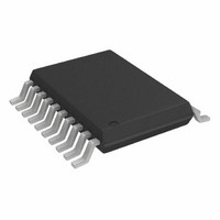
IC,Digital Potentiometer,TSSOP,20PIN,PLASTIC
Manufacturer
Analog Devices Inc
Datasheet
1.AD5254BRUZ100.pdf
(32 pages)
Specifications of AD5253BRU100
Taps
64
Resistance (ohms)
100K
Number Of Circuits
4
Temperature Coefficient
650 ppm/°C Typical
Memory Type
Non-Volatile
Interface
I²C, 2-Wire Serial
Voltage - Supply
2.7 V ~ 5.5 V, ±2.25 V ~ 2.75 V
Operating Temperature
-40°C ~ 85°C
Mounting Type
Surface Mount
Package / Case
20-TSSOP
Resistance In Ohms
100K
Lead Free Status / RoHS Status
Contains lead / RoHS non-compliant
Since the digital potentiometer is not ideal, a 75 Ω finite wiper
resistance is present that can easily be seen when the device is
programmed at zero scale. Because of the fine geometric and
interconnects employed by the device, care should be taken to
limit the current conduction between W and B to no more than
±5 mA continuous for a total resistance of 1 kΩ or a pulse of
±20 mA to avoid degradation or possible destruction of the
device. The maximum dc current for AD5253 and AD5254 are
shown in Figure 21 and Figure 22, respectively.
Similar to the mechanical potentiometer, the resistance of the
RDAC between Wiper W and Terminal A also produces a
digitally controlled complementary resistance, R
terminals are used, the B terminal can be opened. The R
starts at a maximum value and decreases as the data loaded into
the latch increases in value (see Figure 43. The general equation
for this operation is
The typical distribution of R
matches is about ±0.15% within a given device. On the other
hand, device-to-device matching is process-lot dependent with
a ±20% tolerance.
100
AD5253: RWA(D) = [(64 – D)/64] × RAB + 75 Ω
AD5254: RWA(D) = [(256 – D)/256] × RAB + 75 Ω
75
50
25
0
0
Figure 43. AD5253 R
R
10
WA
D (Code in Decimal)
WA
(D) and R
AB
32
from channel-to-channel
WB
(D) vs. Decimal Code
R
48
WB
WA
. When these
63
WA
Rev. B | Page 25 of 32
(3)
(4)
PROGRAMMABLE POTENTIOMETER OPERATION
If all three terminals are used, the operation is called potenti-
ometer mode (see Figure 44); the most common configuration
is the voltage divider operation.
If the wiper resistance is ignored, the transfer function is simply
A more accurate calculation that includes the wiper resistance
effect is
where 2
Unlike in rheostat mode operation, where the tolerance is high,
potentiometer mode operation yields an almost ratiometric
function of D/2
R
Similarly, the ratiometric adjustment also reduces the
temperature coefficient effect to 50 ppm/°C, except at low value
codes where R
Potentiometer mode operations include other applications such
as op amp input, feedback-resistor networks, and other voltage-
scaling applications. The A, W, and B terminals can, in fact, be
input or output terminals, provided that |V
not exceed V
W
terms. Therefore, the tolerance effect is almost cancelled.
AD5253:
AD5254:
V
W
N
(
is the number of steps.
D
)
=
Figure 44. Potentiometer Mode Configuration
DD
W
V
V
2
N
to V
V
D
W
W
R
dominates.
N
I
with a relatively small error contributed by the
AB
=
=
R
SS
AB
+
64
256
D
.
D
2
+
×
R
×
R
V
W
V
A
B
W
AB
AB
V
+
+
A
V
V
B
W
B
AD5253/AD5254
V
C
A
|, |V
W
|, and |V
B
| do
(5)
(6)
(7)


