AD5381BSTZ-3 Analog Devices Inc, AD5381BSTZ-3 Datasheet - Page 31

AD5381BSTZ-3
Manufacturer Part Number
AD5381BSTZ-3
Description
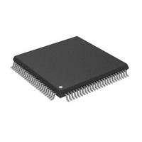
IC,D/A CONVERTER,40-CHANNEL,12-BIT,QFP,100PIN
Manufacturer
Analog Devices Inc
Datasheet
1.AD5381BSTZ-5.pdf
(40 pages)
Specifications of AD5381BSTZ-3
Design Resources
40 Channels of Programmable Voltage with Excellent Temperature Drift Performance Using AD5381 (CN0010) AD5381 Channel Monitor Function (CN0013)
Settling Time
6µs
Number Of Bits
12
Data Interface
Serial, Parallel
Number Of Converters
40
Voltage Supply Source
Single Supply
Power Dissipation (max)
80mW
Operating Temperature
-40°C ~ 85°C
Mounting Type
Surface Mount
Package / Case
100-LQFP
Lead Free Status / RoHS Status
Lead free / RoHS Compliant
For Use With
EVAL-AD5381EB - BOARD EVAL FOR AD5381
Lead Free Status / RoHS Status
Lead free / RoHS Compliant
Available stocks
Company
Part Number
Manufacturer
Quantity
Price
Company:
Part Number:
AD5381BSTZ-3
Manufacturer:
AD
Quantity:
30
Company:
Part Number:
AD5381BSTZ-3
Manufacturer:
Analog Devices Inc
Quantity:
10 000
Part Number:
AD5381BSTZ-3
Manufacturer:
ADI/亚德诺
Quantity:
20 000
Company:
Part Number:
AD5381BSTZ-3-REEL
Manufacturer:
Analog Devices Inc
Quantity:
10 000
MICROPROCESSOR INTERFACING
Parallel Interface
The AD5381 can be interfaced to a variety of 16-bit microcon-
trollers or DSP processors. Figure 35 shows the AD5381 family
interfaced to a generic 16-bit microcontroller/DSP processor.
The lower address lines from the processor are connected to A0
to A5 on the AD5381. The upper address lines are decoded to
provide a CS , LDAC signal for the AD5381. The fast interface
timing of the AD5381 allows direct interface to a wide variety
of microcontrollers and DSPs, as shown in Figure 35.
AD5381 to MC68HC11
The serial peripheral interface (SPI) on the MC68HC11 is
configured for master mode (MSTR = 1), clock polarity bit
(CPOL) = 0, and the clock phase bit (CPHA) = 1. The SPI is
configured by writing to the SPI control register (SPCR)—see
the MC68HC11 user manual. SCK of the MC68HC11 drives the
SCLK of the AD5381, the MOSI output drives the serial data
line (D
D
OUT
. The SYNC signal is derived from a port line (PC7).
IN
) of the AD5381, and the MISO input is driven from
1
ADDITIONAL PINS OMITTED FOR CLARITY.
DSP PROCESSOR
μ CONTROLLER/
UPPER BITS OF
ADDRESS BUS
DATA
BUS
R/W
D15
D0
A5
A4
A3
A2
A1
A0
1
Figure 35. AD5381-to-Parallel Interface
Rev. B | Page 31 of 40
ADDRESS
DECODE
When data is being transmitted to the AD5381, the SYNC line
is taken low (PC7). Data appearing on the MOSI output is valid
on the falling edge of SCK. Serial data from the MC68HC11 is
transmitted in 8-bit bytes with only eight falling clock edges
occurring in the transmit cycle.
MC68HC11
REG1
REG0
D11
D0
CS
LDAC
A5
A4
A3
A2
A1
A0
WR
MISO
MOSI
SCK
PC7
Figure 34. AD5381-to-MC68HC11 Interface
AD5381
DVDD
SER/PAR
RESET
SDO
DIN
SCLK
SYNC
SPI/I
AD5381
2
C
AD5381


