AD569BD Analog Devices Inc, AD569BD Datasheet
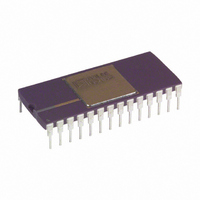
IC,D/A CONVERTER,SINGLE,16-BIT,BICMOS,DIP,28PIN

AD569BD

Manufacturer Part Number
AD569BD
Description
IC,D/A CONVERTER,SINGLE,16-BIT,BICMOS,DIP,28PIN
Manufacturer
Analog Devices Inc
Datasheet

Specifications of AD569BD

Rohs Status
RoHS non-compliant
Settling Time
4µs
Number Of Bits
16
Data Interface
Parallel
Number Of Converters
1
Voltage Supply Source
Dual ±
Operating Temperature
-25°C ~ 85°C
Mounting Type
Through Hole
Package / Case
28-CDIP (0.600", 15.24mm)
Power Dissipation (max)
-
Lead Free Status / RoHS Status

Available stocks

Company
Part Number
Manufacturer
Quantity
Price
Part Number:
AD569BD
Manufacturer:
TI
Quantity:
32
a
PRODUCT DESCRIPTION
The AD569 is a monolithic 16-bit digital-to-analog converter
(DAC) manufactured in Analog Devices’ BiMOS II process.
BiMOS II allows the fabrication of low power CMOS logic
functions on the same chip as high precision bipolar linear cir-
cuitry. The AD569 chip includes two resistor strings, selector
switches decoding logic, buffer amplifiers, and double-buffered
input latches.
The AD569’s voltage-segmented architecture insures 16-bit
monotonicity over time and temperature. Integral nonlinearity is
maintained at 0.01%, while differential nonlinearity is
voltage output settling time of 3 s to within 0.001% for a
full-scale step.
The reference input voltage which determines the output range
can be either unipolar or bipolar. Nominal reference range is
provided for high accuracy applications. The AD569 can oper-
ate with an ac reference in multiplying applications.
Data may be loaded into the AD569’s input latches from 8- and
16-bit buses. The double-buffered structure simplifies 8-bit bus
interfacing and allows multiple DACs to be loaded asynchro-
nously and updated simultaneously. Four TTL/LSTTL/5 V
CMOS-compatible signals control the latches: CS, LBE, HBE,
and LDAC
The AD569 is available in five grades: J and K versions are
specified from 0 C to +70 C and are packaged in a 28-pin plas-
tic DIP and 28-pin PLCC package; AD and BD versions are
specified from –25 C to +85 C and are packaged in a 28-pin
ceramic DIP. The SD version, also in a 28-pin ceramic DIP, is
specified from –55 C to +125 C.
REV. A
Information furnished by Analog Devices is believed to be accurate and
reliable. However, no responsibility is assumed by Analog Devices for its
use, nor for any infringements of patents or other rights of third parties
which may result from its use. No license is granted by implication or
otherwise under any patent or patent rights of Analog Devices.
0.0004%. The on-chip, high-speed buffer amplifiers provide a
5 V and separate reference force and sense connections are
FEATURES
Guaranteed 16-Bit Monotonicity
Monolithic BiMOS II Construction
8- and 16-Bit Bus Compatibility
3 s Settling to 16 Bits
Low Drift
Low Power
Low Noise
APPLICATIONS
Robotics
Closed-Loop Positioning
High-Resolution ADCs
Microprocessor-Based Process Control
MIL-STD-883 Compliant Versions Available
0.01% Typical Nonlinearity
PRODUCT HIGHLIGHTS
1. Monotonicity to 16 bits is insured by the AD569’s voltage-
2. The output range is ratiometric to an external reference or ac
3. The AD569’s versatile data input structure allows loading
4. The on-chip output buffer amplifier can supply 5 V into a
5. Kelvin connections to the reference inputs preserve the gain
6. The AD569 is available in versions compliant with MIL-STD-
One Technology Way, P.O. Box 9106, Norwood, MA 02062-9106, U.S.A.
Tel: 617/329-4700
segmented architecture.
signal. Gain error and gain drift of the AD569 are negligible.
from 8- and 16-bit buses.
1 k load, and can drive capacitive loads of up to 1000 pF.
and offset accuracy of the transfer function in the presence of
wiring resistances and ground currents.
883. Refer to the Analog Devices Military Products Data-
book or current AD569/883B data sheet for detailed
specifications.
Voltage Output D/A Converter
FUNCTIONAL BLOCK DIAGRAM
16-Bit Monotonic
AD569
Fax: 617/326-8703

Related parts for AD569BD

AD569BD Summary of contents

Page 1

FEATURES Guaranteed 16-Bit Monotonicity Monolithic BiMOS II Construction 0.01% Typical Nonlinearity 8- and 16-Bit Bus Compatibility 3 s Settling to 16 Bits Low Drift Low Power Low Noise APPLICATIONS Robotics Closed-Loop Positioning High-Resolution ADCs Microprocessor-Based Process Control MIL-STD-883 Compliant ...

Page 2

AD569–SPECIFICATIONS Model AD569JN/JP/AD Parameter Min RESOLUTION LOGIC INPUTS V (Logic “l”) 2 (Logic “0” 5 TRANSFER FUNCTION CHARACTERISTICS Integral Nonlinearity ...

Page 3

AC PERFORMANCE CHARACTERISTICS These characteristics are included for Design Guidance Only and are not subject to test +12 V; –V = – – REF Parameter Limit Output Voltage Settling 5 (Time ...

Page 4

... AD569JP 0.04% AD569KN 0.024% AD569KP 0.024% AD569AD 0.04% AD569BD 0.024% AD569SD 0.04% NOTES 1 For details on grade and package offerings screened in accordance with MIL-STD-883, refer to the Analog Devices Military Products Databook or current AD569/883B data sheet Ceramic DIP Plastic DIP Plastic Leaded Chip Carrier. ...

Page 5

FUNCTIONAL DESCRIPTION The AD569 consists of two resistor strings, each of which is di- vided into 256 equal segments (see Figure 3). The 8 MSBs of the digital input word select one of the 256 segments on the first string. ...

Page 6

AD569 Figure 5. Typical DNL at Segment Boundary Transitions a. Segment 1 b. Segment 256 Figure 6. Typical DNL Within Segments MULTIPLYING FEEDTHROUGH ERROR: This is the error due to capacitive feedthrough from the reference to the output with the ...

Page 7

Zener diode fail (a short circuit would be the most likely failure), the supply voltage decreases. This differs from the situation where the diode is used as a series regulator. In that case, a failure ...

Page 8

AD569 Figure 9. MSB Resistor Divider Figures 11, 12, and 13 show reference configurations for various output ranges. As shown in Figure 11, the pin-programmable AD588 can be connected to provides tracking 5 V outputs with 1-3ppm/ C temperature stability. ...

Page 9

MULTIPLYING PERFORMANCE Figure 14 illustrates the gain and phase characteristics of the AD569 when operated in the multiplying mode. Full-power bandwidth is shown in Figure 14a and the corresponding phase shift is shown in Figure 14b. Performance is plotted for ...

Page 10

AD569 under worst-case conditions (hex input code 0000), feedthrough remains below –100 reference frequencies kHz. Figure 16. Multiplying Feedthrough BYPASSING AND GROUNDING RULES It is generally considered good engineering practice to use bypass capacitors ...

Page 11

Simple Interface b. Fast Interface Figure 20. 8-Bit Microprocessor Interface 8-Bit Microprocessor Interfaces Since 8-bit microprocessors require two write cycles to provide the AD569’s 16-bit input, the DAC register must be utilized most often loaded as the ...

Page 12

AD569 Preceding the second flash, the residue signal must be amplified by a factor of 256. The OP37 provides a gain of 25.6 and the AD630 provides another gain of 10. In this case, the AD630 acts as a gain ...

Related keywords