AD625AD Analog Devices Inc, AD625AD Datasheet - Page 11
AD625AD
Manufacturer Part Number
AD625AD
Description
Instrumentation Amplifier IC
Manufacturer
Analog Devices Inc
Datasheet
1.AD625KNZ.pdf
(15 pages)
Specifications of AD625AD
Gain Max, V/v
10000
Input Offset Voltage Max
200V
Supply Voltage Max
18V
Mounting Type
Through Hole
Supply Voltage Min
6V
Gain Min, V/v
1
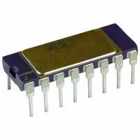
Package / Case
16-CDIP
Rohs Status
RoHS non-compliant
Amplifier Type
Instrumentation
Number Of Circuits
1
Slew Rate
5 V/µs
Gain Bandwidth Product
25MHz
-3db Bandwidth
650kHz
Current - Input Bias
30nA
Voltage - Input Offset
50µV
Current - Supply
3.5mA
Voltage - Supply, Single/dual (±)
±6 V ~ 18 V
Operating Temperature
-40°C ~ 85°C
Output Type
-
Current - Output / Channel
-
Lead Free Status / RoHS Status
Available stocks
Company
Part Number
Manufacturer
Quantity
Price

Company:
Part Number:
AD625ADZ
Manufacturer:
AKM
Quantity:
1 400
Company:
Part Number:
AD625ADZ
Manufacturer:
Analog Devices Inc
Quantity:
135


Offset voltage and offset voltage drift each have two compo-
nents: input and output. Input offset is that component of offset
that is generated at the input stage. Measured at the output it is
directly proportional to gain, i.e., input offset as measured at the
output at G = 100 is 100 times greater than that measured at
G = 1. Output offset is generated at the output and is constant
for all gains.
The input offset and drift are multiplied by the gain, while the
output terms are independent of gain, therefore, input errors
dominate at high gains and output errors dominate at low gains.
The output offset voltage (and drift) is normally specified at
G = 1 (where input effects are insignificant), while input offset
(and drift) is given at a high gain (where output effects are negli-
gible). All input-related parameters are specified referred to the
input (RTI) which is to say that the effect on the output is “G”
times larger. Offset voltage vs. power supply is also specified as
an RTI error.
By separating these errors, one can evaluate the total error inde-
pendent of the gain. For a given gain, both errors can be com-
bined to give a total error referred to the input (RTI) or output
(RTO) by the following formula:
Total Error RTI = input error + (output error/gain)
Total Error RTO = (Gain × input error) + output error
The AD625 provides for both input and output offset voltage
adjustment. This simplifies nulling in very high precision appli-
cations and minimizes offset voltage effects in switched gain
applications. In such applications the input offset is adjusted
first at the highest programmed gain, then the output offset is
adjusted at G = 1. If only a single null is desired, the input offset
null should be used. The most additional drift when using only
the input offset null is 0.9 µV/°C, RTO.
COMMON-MODE REJECTION
Common-mode rejection is a measure of the change in output
voltage when both inputs are changed by equal amounts. These
specifications are usually given for a full-range input voltage
change and a specified source imbalance.
In an instrumentation amplifier, degradation of common-mode
rejection is caused by a differential phase shift due to differences
SIGNAL
INPUT
+V
S
AD7502
–V
S
+V
AD625
S
–V
S
HOLD
CAP
in distributed stray capacitances. In many applications shielded
cables are used to minimize noise. This technique can create
common-mode rejection errors unless the shield is properly
driven. Figures 32 and 33 show active data guards which are
configured to improve ac common-mode rejection by “boot-
strapping” the capacitances of the input cabling, thus minimiz-
ing differential phase shift.
GROUNDING
In order to isolate low level analog signals from a noisy digital
environment, many data-acquisition components have two or
more ground pins. These grounds must eventually be tied to-
gether at one point. It would be convenient to use a single
ground line, however, current through ground wires and pc runs
of the circuit card can cause hundreds of millivolts of error.
Therefore, separate ground returns should be provided to mini-
mize the current flow from the sensitive points to the system
ground (see Figure 34). Since the AD625 output voltage is
developed with respect to the potential on the reference termi-
nal, it can solve many grounding problems.
SAMPLE
–V
AD583
HOLD
AND
S
+V
S
100
100
ANALOG
STATUS
OUT
+V
–V
+INPUT
–INPUT
AD712
S
S
100
+INPUT
–INPUT
CONVERTER
AD574A
AD711
–V
A/D
S
ANALOG POWER
R
R
R
G
F
F
GROUND
COMMON
DIGITAL
R
R
R
G
F
F
V
AD625
LOGIC
+V
–V
AD625
S
S
–V
+V
S
S
SENSE
REFERENCE
AD625
REFERENCE
SENSE
V
OUT
V
OUT
Related parts for AD625AD
Image
Part Number
Description
Manufacturer
Datasheet
Request
R

Part Number:
Description:
DPG2 EVAL ADAPTER FOR XILINX BOARDS
Manufacturer:
Analog Devices Inc
Part Number:
Description:
Xilinx FMC Interface
Manufacturer:
Analog Devices Inc
Datasheet:
Part Number:
Description:
Xilinx FMC Interface
Manufacturer:
Analog Devices Inc
Datasheet:
Part Number:
Description:
Xilinx FMC Interface
Manufacturer:
Analog Devices Inc
Datasheet:
Part Number:
Description:
Xilinx FMC Interface
Manufacturer:
Analog Devices Inc
Datasheet:
Part Number:
Description:
Xilinx FMC Interface
Manufacturer:
Analog Devices Inc
Datasheet:
Part Number:
Description:
Xilinx FMC Interface
Manufacturer:
Analog Devices Inc
Datasheet:
Part Number:
Description:
Xilinx FMC Interface
Manufacturer:
Analog Devices Inc
Datasheet:
Part Number:
Description:
AD CONVERTOR, IC, BIT COUNT FOR PROCESSOR
Manufacturer:
Analog Devices Inc

Part Number:
Description:
±1.7g Dual-Axis IMEMS Accelerometer Evaluation Board
Manufacturer:
Analog Devices Inc
Datasheet:
Part Number:
Description:
Inertial Sensor Evaluation System
Manufacturer:
Analog Devices Inc
Datasheet:
Part Number:
Description:
Manufacturer:
Analog Devices Inc
Datasheet: