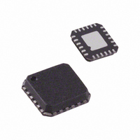
AD7147ACPZ-REEL Analog Devices Inc, AD7147ACPZ-REEL Datasheet - Page 39

AD7147ACPZ-REEL
Manufacturer Part Number
AD7147ACPZ-REEL
Description
IC,Converter, Other/Special/Miscellaneous,LLCC,24PIN
Manufacturer
Analog Devices Inc
Series
CapTouch™r
Type
Capacitive Sensor Controllerr
Datasheet
1.AD7147ACPZ-1500RL7.pdf
(72 pages)
Specifications of AD7147ACPZ-REEL
Resolution (bits)
16 b
Data Interface
Serial, SPI™
Voltage Supply Source
Single Supply
Voltage - Supply
2.6 V ~ 3.6 V
Operating Temperature
-40°C ~ 85°C
Mounting Type
Surface Mount
Package / Case
24-LFCSP
Lead Free Status / RoHS Status
Lead free / RoHS Compliant
For Use With
EVAL-AD7147EBZ - BOARD EVAL FOR AD7147ACPZEVAL-AD7147-1EBZ - BOARD EVAL FOR AD7147ACPZ-1
Sampling Rate (per Second)
-
Lead Free Status / Rohs Status
Compliant
POWER-UP SEQUENCE
To power up the AD7147, use the following sequence when
initially developing the AD7147 and microprocessor serial
interface:
1.
2.
3.
CONVERSION
INTERFACE
AD7147 INT
POWER
SERIAL
STAGE
Turn on the power supplies to the AD7147.
Write to the Bank 2 registers at Address 0x080 through
Address 0x0DF. These registers are contiguous; therefore, a
sequential register write sequence can be applied.
Note that the Bank 2 register values are unique for each
application. Register values come from characterization of
the sensor in the application.
Write to the Bank 1 registers at Address 0x000 through
Address 0x007, outlined as follows. These registers are
contiguous; therefore, a sequential register write sequence
can be applied (see Figure 50 and Figure 55).
Caution: At this time, Address 0x001 must remain set to a
default value of 0x0000 during this contiguous write
operation.
Register values:
Address 0x000 = 0x82B2
Address 0x001 = 0x000
Address 0x002 = 0x3230 (depends on number of
conversion stages used)
Address 0x003 = 0x419
HOST
CONVERSION STAGES DISABLED
0
1
2
Figure 59. Recommended Start-Up Sequence
3
FIRST CONVERSION SEQUENCE
4
5
Rev. B | Page 39 of 72
6
7
8
9
10 11
4.
5.
6.
Address 0x004 = 832
Address 0x005 = interrupt enable register (depends on
required interrupt behavior)
Address 0x006 = interrupt enable register (depends on
required interrupt behavior)
Address 0x007 = interrupt enable register (depends on
required interrupt behavior)
Write to the Bank 1 register, Address 0x001 = 0x0FFF
(depends on number of conversion stages used).
Read back the corresponding interrupt status register at
Address 0x008, Address 0x009, or Address 0x00A. This is
determined by the interrupt output configuration, as
explained in the Interrupt Output section.
Note that the specific registers required to be read back
depend on each application. For buttons, the interrupt
status registers are read back while other sensors read data
back from the AD7147 according to the slider or wheel
algorithm’s requirements. Analog Devices can provide this
information after the user develops the sensor board.
Repeat Step 5 every time INT is asserted.
0
1
2
SECOND CONVERSION
SEQUENCE
9
10 11
0
1
2
THIRD CONVERSION
SEQUENCE
9
10
11
AD7147
0
1


