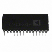
AD760AQ Analog Devices Inc, AD760AQ Datasheet - Page 9

AD760AQ
Manufacturer Part Number
AD760AQ
Description
Digital-Analog Converter IC
Manufacturer
Analog Devices Inc
Series
DACPORT®r
Datasheet
1.AD760AQ.pdf
(12 pages)
Specifications of AD760AQ
Rohs Status
RoHS non-compliant
Settling Time
6µs
Number Of Bits
16
Data Interface
Serial, Parallel
Number Of Converters
1
Voltage Supply Source
Dual ±
Power Dissipation (max)
725mW
Operating Temperature
-40°C ~ 85°C
Mounting Type
Through Hole
Package / Case
28-CDIP (0.600", 15.24mm)
Lead Free Status / RoHS Status
Available stocks
Company
Part Number
Manufacturer
Quantity
Price
Company:
Part Number:
AD760AQZ
Manufacturer:
INTEL
Quantity:
32
REV. A
The digital-to-analog glitch impulse is specified as 15 nV-s typi-
cal. Figure 8c shows the typical glitch impulse characteristic at
the code 011 . . . 111 to 100 . . . 000 transition when loading
the second rank register from the first rank register.
DIGITAL CIRCUIT DETAILS
The AD760 has several “dual-use” pins that allow flexible op-
eration while maintaining the lowest possible pin count and con-
sequently the smallest package size. The following information
is useful when applying the AD760.
The AD760 uses an internal Output Multiplexer to discon-
nect the DAC output from MUX
is uncalibrated or when a calibration sequence is in progress. At
those times MUX
user can force a predetermined output voltage. Refer to the fol-
lowing section for using the output multiplexer.
–400
–200
–600
+10
–10
400
200
600
+20
–20
a. –10 V to +10 V Full-Scale Step Settling
0
0
0
0
0
0
Figure 8. Output Characteristics
OUT
c. D-to-A Glitch Impulse
1
1
b. LSB Step Settling
is switched to MUX
2
2
10
µs
µs
µs
OUT
3
3
(Pin 27) when the device
IN
4
4
(Pin 28) so the
20
5
5
400
200
–400
600
0
–200
–600
–9–
A Power-On-Reset feature senses whenever any power supply
is low enough to jeopardize the integrity of the calibration data
in the RAM. At power-up or in the event of a power supply
transient, CALOK (Pin 1) is low and the MUX
switched to MUX
Self-Calibration is initiated by strobing the CAL pin low (refer
to Figure 1d). The CALOK pin will go low and the MUX
pin is connected to MUX
latch is transparent to allow the CALIBRATION SEQUENCER
to control the MAIN DAC. After successful completion of cali-
bration, the input to the second-rank latch is switched to the
first-rank latch, the DAC is loaded with the contents of the first-
rank latch, V
the first-rank latch, then CALOK will go high, and MUX
switched to V
with the desired data before initiating the calibration. The sec-
ond rank latch, controlled by LDAC, is a transparent latch. As
long as LDAC remains high, changes in the first rank latch will
be reflected in the DAC output immediately.
The status of the calibration may be determined by taking the
HBE pin low. CALOK either switches high if the calibration is
in progress, or CALOK remains low if a power supply voltage
transient has interrupted the calibration and caused the AD760
to be set to the uncalibrated state.
When CLR is strobed, Pin 17 functions as a control input, UNI/
BIP CLR, that determines how the Asynchronous Clear func-
tion works (refer to Figure 1c). If the UNI/BIP CLR pin is a
logic low when CLR is strobed the DAC is set to minus full-
scale; a logic high sets the DAC to midscale. It should be noted
that the clear function clears the DAC Latch but does not clear
the first rank latch. Therefore, the data that remains in the first
rank latch can be reloaded by simply bringing LDAC high
again. Alternately, new data can be loaded into the first rank
latch if desired.
Serial Mode Operation is enabled by bringing the SER (Pin
19) low. This changes the function of DB0 (Pin 14) to that of
the serial input pin, SIN. The function of DB1 (Pin 13) also
changes to a control input, MSB/LSB that determines which bit
is to be loaded first.
Sixteen or Eighteen-Bit Operation is selected with another
dual use pin. DB2 (Pin 12) changes to a control input, 18/16-
SERIAL, that selects whether 16-bit or 18-bit serial data is to be
used. For 16-bit operation the data inputs, Pins 7–12, should be
tied low. For 18-bit operation Pin 12 must be tied high.
Data is clocked into the input shift register on the rising edge of
CS as shown in Figure 1b. The data is then resident in the first
rank latch and can be loaded into the DAC by taking the LDAC
pin high. This will cause the DAC to change to the appropriate
output value. In serial mode the byte controls HBE (Pin 18)
and LBE (Pin 17) are disabled. Pin 17 can be tied to a logic
high or low depending on how the user wants the asynchronous
clear function to work. The Serial Out pin (S
to daisy chain several DACs together in multi-DAC applications
to minimize the number of control lines required. The first rank
latch simply acts as a shift register, and repeated strobing of CS
will shift the data out through S
Each DAC in the chain will require its own LDAC signal unless
all of the DACs are to be updated simultaneously.
OUT
OUT
settles to the value represented by the data in
. Therefore the user should program the DAC
IN
.
IN
. During calibration, the second-rank
OUT
and into the next DAC.
OUT
OUT
AD760
) can be used
pin is
OUT
OUT
is


