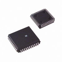
AD7716BPZ Analog Devices Inc, AD7716BPZ Datasheet - Page 5

AD7716BPZ
Manufacturer Part Number
AD7716BPZ
Description
4-CHNL S-D ADC
Manufacturer
Analog Devices Inc
Datasheet
1.AD7716BP-REEL.pdf
(16 pages)
Specifications of AD7716BPZ
Number Of Bits
22
Sampling Rate (per Second)
2.23k
Data Interface
Serial
Number Of Converters
4
Power Dissipation (max)
50mW
Voltage Supply Source
Analog and Digital, Dual ±
Operating Temperature
-40°C ~ 85°C
Mounting Type
Surface Mount
Package / Case
44-PLCC
Lead Free Status / RoHS Status
Lead free / RoHS Compliant
For Use With
EVAL-AD7716EBZ - BOARD EVAL FOR AD7716
Lead Free Status / RoHS Status
Lead free / RoHS Compliant
Available stocks
Company
Part Number
Manufacturer
Quantity
Price
Company:
Part Number:
AD7716BPZ
Manufacturer:
ST
Quantity:
2 100
Company:
Part Number:
AD7716BPZ
Manufacturer:
Analog Devices Inc
Quantity:
10 000
SLAVE MODE TIMING CHARACTERISTICS
f
Parameter
f
t
t
t
t
t
t
t
t
t
t
t
t
NOTES
1
2
3
4
5
6
7
REV. A
back to remove the effects of charging or discharging the 100 pF capacitor. This means that the time quoted in the timing characteristics is the true bus relinquish
Sample tested at +25 C to ensure compliance. All input signals are specified with tr = tf = 5 ns (10% to 90% of 5 V) and timed from a voltage level of 1.6 V.
See Figures 1 and 4.
CLKIN duty cycle range is 40% to 60%.
The AD7716 is production tested with f
Specified using 10% and 90% points on waveform of interest.
t
t
CLKIN
CLKIN
r
f
23
24
25
26
27
28
29
30
31
32
time of the part and as such is independent of external bus loading capacitances.
5
28
30
5
6
7
is measured with the load circuit of Figure 1 and defined as the time required for an output to cross 0.8 V or 2.4 V.
is derived from the measured time taken by the data outputs to change 0.5 V when loaded with the circuit of Figure 1. The measured number is then extrapolated
= 8 MHz; Input Levels: Logic 0 = 0 V, Logic 1 = DV
3, 4
CASCOUT (O)
SDATA (O)
CASCIN (I)
SCLK (I)
RFS (I)
(B Version)
400
8
40
40
1/f
50
125
1/f
30
50
50
50
0
60
2/f
CLKIN
CLKIN
CLKIN
t
23
CLKIN
+30
t
26
at 8 MHz in the slave mode. It is guaranteed by characterization to operate at 400 kHz.
t
28
Figure 4. Slave Mode Timing Diagram
DD
t
DB31
27
CH1
; unless otherwise noted)
t
24
t
Units
kHz min
MHz max
ns max
ns max
ns min
ns min
ns min
ns min
ns min
ns max
ns min
ns max
ns min
ns max
ns max
24
1, 2
DB30
CH1
(AV
–5–
t
25
DB29
DD
CH1
= DV
DD
DB28
CH1
= +5 V
DB27
CH1
Conditions/Comments
CLKIN Frequency
Digital Output Rise Time. Typically 20 ns
Digital Output Fall Time. Typically 20 ns
CASCIN Pulse Width
SCLK Width
SCLK Period
CASCIN High to RFS Setup Time
RFS Low to SCLK High Setup Time
SCLK High to SDATA Valid Delay
RFS Hold Time After SCLK High
SCLK High to SDATA High Impedance Delay
SCLK High to CASCOUT High Delay.
CASCOUT Pulse Width
5%; AV
DB2
CH4
SS
t
DB1
CH4
31
= –5 V
DB0
CH4
t
32
5%; AGND = DGND = 0 V;
t
t
30
29
AD7716


