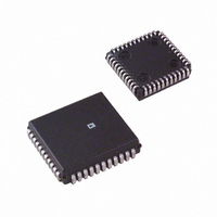
AD7716BPZ Analog Devices Inc, AD7716BPZ Datasheet - Page 7

AD7716BPZ
Manufacturer Part Number
AD7716BPZ
Description
4-CHNL S-D ADC
Manufacturer
Analog Devices Inc
Datasheet
1.AD7716BP-REEL.pdf
(16 pages)
Specifications of AD7716BPZ
Number Of Bits
22
Sampling Rate (per Second)
2.23k
Data Interface
Serial
Number Of Converters
4
Power Dissipation (max)
50mW
Voltage Supply Source
Analog and Digital, Dual ±
Operating Temperature
-40°C ~ 85°C
Mounting Type
Surface Mount
Package / Case
44-PLCC
Lead Free Status / RoHS Status
Lead free / RoHS Compliant
For Use With
EVAL-AD7716EBZ - BOARD EVAL FOR AD7716
Lead Free Status / RoHS Status
Lead free / RoHS Compliant
Available stocks
Company
Part Number
Manufacturer
Quantity
Price
Company:
Part Number:
AD7716BPZ
Manufacturer:
ST
Quantity:
2 100
Company:
Part Number:
AD7716BPZ
Manufacturer:
Analog Devices Inc
Quantity:
10 000
Pin
AV
DV
AV
RESET
A0–A2
CLKIN
CLKOUT
MODE
CASCIN
CASCOUT
RFS
SDATA
SCLK
DRDY
TFS
D
D
V
AGND
DGND
A
REV. A
REF
IN
IN
OUT
DD
SS
DD
1–A
1
1, D
IN
4
OUT
2
Description
Analog Positive Supply, +5 V Nominal. This supplies +ve power to the analog modulators. AV
must be tied together externally.
Digital Positive Supply, +5 V Nominal. This supplies +ve power to the digital filter and input/output registers.
Analog Negative Supply, –5 V nominal. This supplies –ve power to the analog modulators.
A high pulse on this input pin synchronizes the sampling point on the four input channels. It can be used in a
multichannel system to ensure simultaneous sampling. This also resets the digital interface to a known state.
The three address input pins, A0, A1 and A2 give the device a unique address. This information is contained in
the output data stream from the device.
Clock Input for External Clock.
Clock Output which is used to generate an internal master clock by connecting a crystal between CLKOUT and
CLKIN. If an external clock is used then CLKOUT is not connected.
This digital input determines the device interface mode. If it is hardwired low, then the Master Mode interface is
enabled whereas if it is high, the Slave Mode interface is enabled.
This is an active-high, level-triggered digital input which is used to enable the output data stream. This input
may be used to cascade several devices in a multichannel system.
Digital output which goes high at the end of a complete 4-channel data transfer. This can be connected to the
CASCIN of the next device in a multichannel system to ensure proper control of the data transfer.
Receive Frame Synchronization signal for the serial output data stream. This can be an input or output depending
on the interface mode.
Serial Data Input/Output Pin.
Serial Clock Input/Output. The SCLK pin is configured as an input or output, depending on the state of the
Mode pin.
Data Ready Output. A falling edge indicates that a new word is available for transmission. It will return high
when 4, 32-bit words have been transmitted. It also goes high for one clock cycle, when a new word is being
loaded into the output register. Data should not be read during this period.
Transmit Frame Sync input for programming the on-chip Control Register.
Digital Data Input. This is contained in the digital data stream sent from the device.
Digital Outputs. These two digital outputs can be programmed from the on-chip Control Register. They can
be used to control calibration signals at the front end.
Reference Input, Nominally 2.5 V.
Analog Ground. Ground reference for analog circuitry.
Digital Ground. Ground return for digital circuitry.
Analog Input Pins. The analog input range is 2.5 V.
PIN DESCRIPTION
–7–
DD
& DV
AD7716
DD


