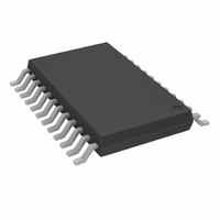
AD7731BRUZ-REEL Analog Devices Inc, AD7731BRUZ-REEL Datasheet - Page 2

AD7731BRUZ-REEL
Manufacturer Part Number
AD7731BRUZ-REEL
Description
24-BIT SIGMA DELTA ADC I.C.
Manufacturer
Analog Devices Inc
Datasheet
1.AD7731BRUZ.pdf
(44 pages)
Specifications of AD7731BRUZ-REEL
Number Of Bits
24
Sampling Rate (per Second)
6.4k
Data Interface
DSP, Serial, SPI™
Number Of Converters
1
Power Dissipation (max)
125mW
Voltage Supply Source
Analog and Digital
Operating Temperature
-40°C ~ 85°C
Mounting Type
Surface Mount
Package / Case
24-TSSOP (0.173", 4.40mm Width)
Lead Free Status / RoHS Status
Lead free / RoHS Compliant
For Use With
EVAL-AD7731EBZ - BOARD EVALUATION FOR AD7731
Lead Free Status / RoHS Status
Lead free / RoHS Compliant
Available stocks
Company
Part Number
Manufacturer
Quantity
Price
Company:
Part Number:
AD7731BRUZ-REEL7
Manufacturer:
ADI
Quantity:
1 000
Part Number:
AD7731BRUZ-REEL7
Manufacturer:
ADI/亚德诺
Quantity:
20 000
AD7731–SPECIFICATIONS
Parameter
STATIC PERFORMANCE (CHP = 0)
STATIC PERFORMANCE (CHP = 1)
ANALOG INPUTS/REFERENCE INPUTS
No Missing Codes
Output Noise and Update Rates
Integral Nonlinearity
Offset Error
Offset Drift vs. Temperature
Offset Drift vs. Time
Positive Full-Scale Error
Positive Full-Scale Drift vs. Temp
Positive Full-Scale Drift vs. Time
Gain Error
Gain Drift vs. Temperature
Gain Drift vs. Time
Bipolar Negative Full-Scale Error
Negative Full-Scale Drift vs. Temp
Power Supply Rejection
Power Supply Rejection
Common-Mode Rejection (CMR)
Analog Input DC Bias Current
Analog Input DC Bias Current Drift
Analog Input DC Offset Current
Analog Input DC Offset Current Drift
Normal Mode 50 Hz/60 Hz Rejection
Common-Mode 50 Hz/60 Hz Rejection
Analog Inputs
On AIN
On AIN
On REF IN
On AIN
On AIN
On REF IN
Differential Input Voltage Ranges
2, 9
9
2
2
5
5
5
5
11
11
11
11
2, 6
6
2, 7, 10
7, 10
2
2
2
2
5
2
5
2, 7, 8
7, 8
11
11
2, 7
12
2
2
2
2
2
B Version
24
See Tables I and II
15
See Note 4
0.5
1/2/5
2.5
See Note 4
0.6
1.5/3/6
3
See Note 4
2
10
See Note 4
1
90
60
95
85
120
60
150
30
100
24
See Tables III and IV
15
See Note 4
5
25
See Note 4
2
10
See Note 4
2
10
See Note 4
2
110
85
110
85
120
50
100
10
50
88
120
0 to +20 or 20
0 to +40 or 40
0 to +80 or 80
0 to +160 or 160
0 to +320 or 320
0 to +640 or 640
0 to +1.28 or 1.28
(AV
DGND = 0 V; f
1
DD
= +5 V, DV
CLK IN
–2–
Units
Bits min
ppm of FSR max
ppm/ C typ
ppm/1000 Hr
dB typ
dB typ
dB typ
dB typ
dB typ
nA max
pA/ C typ
nA max
pA/ C typ
Bits min
ppm of FSR max
nV/ C typ
nV/1000 Hr typ
ppm of FS/ C max
ppm of FS/1000 Hr
ppm/ C max
ppm/1000 Hr
ppm of FS/ C max
dB typ
dB typ
dB typ
dB typ
dB typ
nA max
pA/ C typ
nA max
pA/ C typ
dB min
dB min
mV nom
mV nom
mV nom
mV nom
mV nom
mV nom
V nom
DD
V/ C typ
V/ C typ
V/ C typ
V/ C typ
V/1000 Hr
V/ C typ
V/1000 Hr
= 4.9152 MHz. All specifications T
= +3 V or +5 V; REF IN(+) = +2.5 V; REF IN(–) = AGND; AGND =
Conditions/Comments
SKIP = 0
Offset Error and Offset Drift Refer to Both
Input Range = 20 mV, 40 mV, 80 mV, 160 mV
Input Range = 320 mV/640 mV/1.28 V
Input Range = 20 mV, 40 mV, 80 mV, 160 mV
Input Range = 320 mV/640 mV/1.28 V
Input Range = 20 mV
Input Range = 1.28 V
At DC. Input Range = 20 mV
At DC. Input Range = 1.28 V
Offset Error and Offset Drift Refer to Both
Unipolar Offset and Bipolar Zero Errors
Input Range = 20 mV
Input Range = 1.28 V
At DC. Input Range = 20 mV
At DC. Input Range = 1.28 V
50 Hz/60 Hz 1 Hz. SKIP = 0
50 Hz/60 Hz 1 Hz. SKIP = 0
Assuming 2.5 V or 5 V Reference with HIREF
Bit Set Appropriately
RN2, RN1, RN0 of Mode Register = 0, 0, 1
RN2, RN1, RN0 of Mode Register = 0, 1, 0
RN2, RN1, RN0 of Mode Register = 0, 1, 1
RN2, RN1, RN0 of Mode Register = 1, 0, 0
RN2, RN1, RN0 of Mode Register = 1, 0, 1
RN2, RN1, RN0 of Mode Register = 1, 1, 0
RN2, RN1, RN0 of Mode Register = 1, 1, 1
3
MIN
to T
MAX
unless otherwise noted.)
REV. 0
REV. A


