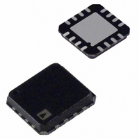
AD8270ACPZ-RL Analog Devices Inc, AD8270ACPZ-RL Datasheet

AD8270ACPZ-RL
Specifications of AD8270ACPZ-RL
Related parts for AD8270ACPZ-RL
AD8270ACPZ-RL Summary of contents
Page 1
FEATURES With no external resistors Difference amplifier: gains of 0. Single ended amplifiers: over 40 different gains Set reference voltage at midsupply Excellent ac specifications 15 MHz bandwidth 30 V/μs slew rate High accuracy dc performance 0.08% ...
Page 2
AD8270 TABLE OF CONTENTS Features .............................................................................................. 1 Applications....................................................................................... 1 General Description ......................................................................... 1 Functional Block Diagram .............................................................. 1 Revision History ............................................................................... 2 Specifications..................................................................................... 3 Difference Amplifier Configurations ........................................ 3 Absolute Maximum Ratings............................................................ 5 Thermal Resistance ...................................................................... 5 Maximum Power Dissipation ...
Page 3
SPECIFICATIONS DIFFERENCE AMPLIFIER CONFIGURATIONS V = ± 25° REF A LOAD Table 2. Parameter Conditions DYNAMIC PERFORMANCE Bandwidth Slew Rate Settling Time to 0.01 step on output Settling Time ...
Page 4
AD8270 V = ± 25° REF A LOAD Table 3. Parameter DYNAMIC PERFORMANCE Bandwidth Slew Rate Settling Time to 0.01% Settling Time to 0.001% NOISE/DISTORTION Harmonic Distortion 1 Voltage Noise GAIN ...
Page 5
ABSOLUTE MAXIMUM RATINGS Table 4. Parameter Supply Voltage Output Short-Circuit Current Input Voltage Range Storage Temperature Range Specified Temperature Range Package Glass Transition Temperature (T ESD (Human Body Model) ESD (Charge Device Model) ESD (Machine Model) Stresses above those listed ...
Page 6
AD8270 PIN CONFIGURATION AND FUNCTION DESCRIPTIONS Table 6. Pin Function Descriptions Pin No. Mnemonic Description 1 −IN1A 10 kΩ Resistor Connected to Negative Terminal of Op Amp A. 2 −IN2A 10 kΩ Resistor Connected to Negative Terminal of Op Amp ...
Page 7
TYPICAL PERFORMANCE CHARACTERISTICS V = ± 25°C, difference amplifier configuration, unless otherwise noted 160 140 120 100 –0.9 –0.6 –0.3 0 SYSTEM OFFSET VOLTAGE (mV) Figure 4. Typical Distribution of ...
Page 8
AD8270 6 (0, +5) 4 (–4.3, +2.85) (0, +2.5) 2 (–1.6, +1. ±2 (–1.6, –1.7) –2 (0, –2.5) (–4.3, –2.85) (–4.3, +2.85) –4 (0, –5) –6 –5 –4 –3 –2 – OUTPUT VOLTAGE (V) ...
Page 9
GAIN = 2 5 GAIN = 1 0 GAIN = 0.5 –5 –10 –15 –20 100 1k 10k 100k 1M FREQUENCY (Hz) Figure 16. Gain vs. Frequency 100 90 GAIN = 2, 0.5 80 GAIN = ...
Page 10
AD8270 V = ±15V S 100pF 18pF 0pF 1µs/DIV Figure 22. Small Signal Step Response, Gain = 0 ±15V S 220pF 33pF 0pF 1µs/DIV Figure 23. Small Signal Step Response, Gain = ±15V S 470pF ...
Page 11
V = ±15V ±5V IN 1µs/DIV Figure 28. Large Signal Pulse Response Gain = 0 ±15V ±5V IN 1µs/DIV Figure 29. Large Signal Pulse Response Gain = ±15V S ...
Page 12
AD8270 210 180 150 120 –600 –400 –200 0 V (µV) OSI Figure 34. Typical Distribution of Op Amp Voltage Offset 100 310 315 320 325 330 I (nA) BIAS Figure ...
Page 13
THEORY OF OPERATION 10kΩ 10kΩ 10kΩ –IN1A 1 10kΩ _ –IN2A 2 10kΩ +IN2A 3 + 10kΩ AD8270 +IN1A 4 20kΩ 20kΩ 20kΩ 20kΩ Figure 40. Functional Block Diagram CIRCUIT INFORMATION The AD8270 has two channels, each consisting of a ...
Page 14
AD8270 INPUT VOLTAGE RANGE The AD8270 has a true rail-to-rail input range for the majority of applications. Because most AD8270 configurations divide down the voltage before they reach the internal op amp, the op amp sees only a fraction of ...
Page 15
APPLICATIONS INFORMATION DIFFERENCE AMPLIFIER CONFIGURATIONS The AD8270 can be placed in difference amplifier configurations with gains of 0.5, 1, and 2. Figure 42 through Figure 44 show the difference amplifier configurations, referenced to ground. The AD8270 can also be referred ...
Page 16
AD8270 Table 8. Selected Single-Ended Configurations Electrical Performance Op Amp Closed-Loop Gain Signal Gain −2 3 −1.5 3 −1.4 3 −1.25 3 −1 3 −0.8 3 −0.667 2 −0.6 2 −0.5 2 −0.333 2 −0.25 1.5 −0.2 1.5 −0.125 1.5 ...
Page 17
The AD8270 Specifications section and Typical Performance Characteristics section show the performance of the part primarily when the difference amplifier configuration. To get a good estimate of the performance of the part in a single-ended configuration, refer ...
Page 18
AD8270 DRIVING AN ADC The AD270 high slew rate and drive capability, combined with its dc accuracy, make it a good ADC driver. The AD8270 can drive both single-ended and differential input ADCs. Many converters require the output to be ...
Page 19
... OUTLINE DIMENSIONS PIN 1 INDICATOR 12° MAX 1.00 0.85 0.80 ORDERING GUIDE Model Temperature Range 1 AD8270ACPZ-R7 −40°C to +85°C 1 AD8270ACPZ-RL −40°C to +85°C 1 AD8270ACPZ-WP −40°C to +85° RoHS Compliant Part. 4.00 BSC SQ 0.60 MAX 0.65 BSC TOP 3.75 VIEW BSC SQ 0 ...
Page 20
AD8270 NOTES ©2008 Analog Devices, Inc. All rights reserved. Trademarks and registered trademarks are the property of their respective owners. D06979-0-1/08(0) Rev Page ...


