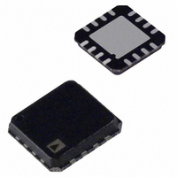
AD8270ACPZ-RL Analog Devices Inc, AD8270ACPZ-RL Datasheet - Page 15

AD8270ACPZ-RL
Manufacturer Part Number
AD8270ACPZ-RL
Description
10MHz, Low Dist Dual Channel Diff Amp
Manufacturer
Analog Devices Inc
Datasheet
1.AD8270ACPZ-WP.pdf
(20 pages)
Specifications of AD8270ACPZ-RL
Amplifier Type
Differential
Number Of Circuits
2
Output Type
Rail-to-Rail
Slew Rate
30 V/µs
Gain Bandwidth Product
20MHz
Current - Input Bias
500pA
Voltage - Input Offset
450µV
Current - Supply
2.3mA
Current - Output / Channel
100mA
Voltage - Supply, Single/dual (±)
5 V ~ 36 V, ±2.5 V ~ 18 V
Operating Temperature
-40°C ~ 85°C
Mounting Type
Surface Mount
Package / Case
16-LFCSP
Lead Free Status / RoHS Status
Lead free / RoHS Compliant
-3db Bandwidth
-
Lead Free Status / RoHS Status
Lead free / RoHS Compliant
APPLICATIONS INFORMATION
DIFFERENCE AMPLIFIER CONFIGURATIONS
The AD8270 can be placed in difference amplifier configurations
with gains of 0.5, 1, and 2. Figure 42 through Figure 44 show the
difference amplifier configurations, referenced to ground. The
AD8270 can also be referred to a combination of reference voltages.
For example, the reference could be set at 2.5 V, using just 5 V
and GND. Some of the possible configurations are shown in
Figure 45 through Figure 47.
The layout for Channel A is shown in Figure 42 through Figure 47.
The layout for Channel B is symmetrical. Table 7 shows the pin
connections for Channel A and Channel B.
Table 7. Pin Connections for Difference Amplifier Configurations
Gain and Reference
Gain of 0.5, Referenced to Ground
Gain of 0.5, Referenced to Midsupply OUT
Gain of 1, Referenced to Ground
Gain of 1, Referenced to Midsupply
Gain of 2, Referenced to Ground
Gain of 2, Referenced to Midsupply
Figure 42. Gain = 0.5 Difference Amplifier, Referenced to Ground
Figure 43. Gain = 1 Difference Amplifier, Referenced to Ground
Figure 44. Gain = 2 Difference Amplifier, Referenced to Ground
–IN
+IN
–IN
+IN
–IN
+IN
NC = NO CONNECT
NC
NC
1
2
3
4
1
2
3
4
1
2
3
4
10kΩ
10kΩ
10kΩ
10kΩ
10kΩ
10kΩ
10kΩ
10kΩ
10kΩ
10kΩ
10kΩ
10kΩ
20kΩ 20kΩ
20kΩ 20kΩ
20kΩ 20kΩ
16
16
16
5
GND
5
GND
5
GND
10kΩ
10kΩ
10kΩ
15
15
15
6
6
6
=
=
=
–IN
+IN
–IN
+IN
–IN
+IN
10kΩ
10kΩ
10kΩ
10kΩ
5kΩ
5kΩ
Pin 1
OUT
−IN
−IN
−IN
−IN
GND
GND
GND
5kΩ
10kΩ
10kΩ
10kΩ
10kΩ
5kΩ
Pin 2
−IN
−IN
NC
NC
−IN
−IN
Pin 3
+IN
NC
+IN
+IN
NC
+IN
Channel A
Rev. 0 | Page 15 of 20
Pin 4
GND
−V
+IN
+IN
+IN
+IN
S
Pin 5
GND
+V
GND
−V
GND
−V
SINGLE-ENDED CONFIGURATIONS
The AD8270 can be configured for a wide variety of single-
ended configurations with gains ranging from −2 to +3.
Table 8 shows a subset of the possible configurations.
Many signal gains have more than one configuration choice,
which allows freedom in choosing the op amp closed-loop gain.
In general, for designs that need to be stable with a large capacitive
load on the output, choose a configuration with high loop gain.
Otherwise, choose a configuration with low loop gain, because
these configurations typically have lower noise, lower offset,
and higher bandwidth.
S
S
S
Figure 45. Gain = 0.5 Difference Amplifier, Referenced to Midsupply
Figure 46. Gain = 1 Difference Amplifier, Referenced to Midsupply
Figure 47. Gain = 2 Difference Amplifier, Referenced to Midsupply
Pin 6
GND
+V
GND
+V
GND
+V
S
S
S
+IN
+IN
–IN
–IN
–IN
+IN
NC = NO CONNECT
NC
NC
–V
S
Pin 12
OUT
−IN
−IN
OUT
−IN
−IN
1
2
3
4
1
2
3
4
1
2
3
4
10kΩ
10kΩ
10kΩ
10kΩ
10kΩ
10kΩ
10kΩ
10kΩ
10kΩ
10kΩ
10kΩ
10kΩ
20kΩ 20kΩ
20kΩ 20kΩ
20kΩ 20kΩ
–V
–V
16
16
16
5
5
5
10kΩ
10kΩ
10kΩ
+V
S
S
+V
+V
S
Pin 11
−IN
−IN
NC
NC
−IN
−IN
15
15
15
6
6
6
S
S
=
=
=
+IN
–IN
–IN
+IN
–IN
+IN
Pin 10
+IN
+IN
NC
NC
+IN
+IN
Channel B
10kΩ
10kΩ
10kΩ
10kΩ
5kΩ
5kΩ
+V
+V
+V
S
S
S
+ –V
2
+ –V
2
+ –V
2
5kΩ
10kΩ
10kΩ
−V
+IN
+IN
Pin 9 Pin 8 Pin 7
GND
+IN
+IN
10kΩ
10kΩ
S
S
S
5kΩ
S
GND
+V
GND
−V
GND
−V
AD8270
S
S
S
GND
+V
GND
+V
+V
GND
S
S
S


