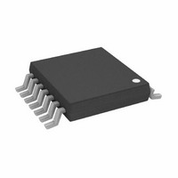
AD8304ARUZ-RL7 Analog Devices Inc, AD8304ARUZ-RL7 Datasheet - Page 16

AD8304ARUZ-RL7
Manufacturer Part Number
AD8304ARUZ-RL7
Description
IC,Level Detector,TSSOP,14PIN,PLASTIC
Manufacturer
Analog Devices Inc
Type
Logarithmic Converterr
Datasheet
1.AD8304ARUZ-RL7.pdf
(20 pages)
Specifications of AD8304ARUZ-RL7
Design Resources
Interfacing ADL5315 to Translinear Logarithmic Amplifier (CN0056) Interfacing ADL5317 High Side Current Mirror to a Translinear Logarithmic Amplifier in an Avalanche Photodiode Power Detector
Applications
Fiber Optics
Mounting Type
Surface Mount
Package / Case
14-TSSOP
Lead Free Status / RoHS Status
Lead free / RoHS Compliant
Available stocks
Company
Part Number
Manufacturer
Quantity
Price
Company:
Part Number:
AD8304ARUZ-RL7
Manufacturer:
AME
Quantity:
14 500
AD8304
When the gain is set to 13 (R
directly to BFIN, in which case the starting point for the output
response is at 4 V. However, since the slope in this case is only
–0.2 V/decade, the full current range will only take the output
NC = NO CONNECT
R1
750
C1
1nF
10nF
I
PD
NC
Figure 15. Using the Buffer to Invert the Polarity
of the Slope
6
3
4
5
AD8304
VPDB
VSUM
VSUM
INPT
V
N
(–0.5V TO –3V)
VPS2
1
PDB
VNEG
10
PWDN
~10k
25k
C2
1nF
B
ACOM
NC = NO CONNECT
COMPENSATION
BIAS
TEMPERATURE
1nF
750
= 5 kΩ) the 2 V V
10nF
2
I
PD
1k
NC
14
NC = NO CONNECT
I
SRC
NC
6
3
4
5
AD8304
VSUM
VSUM
VPDB
INPT
4
0.5V
6
3
5
VPS1
AD8304
VPDB
VSUM
VSUM
INPT
V
VREF
VOUT
VPS2
VNEG
N
12
Figure 16. Calibrated Level Comparator
Figure 17. Multidecade Current Source
5k
(–0.5V TO –5V)
VPS2
1
PDB
VNEG
11
10
REF
BFNG
1
BFIN
PDB
10
can be tied
PWDN
13
~10k
7
8
9
V
V
VLOG
VREF
PWDN
P
OFS
~10k
COMPENSATION
ACOM
TEMPERATURE
BIAS
ACOM
2
COMPENSATION
V
BIAS
TEMPERATURE
RB
OUT
2
14
–16–
14
VPS1
0.5V
down by 1.6 V. Clearly, a higher slope (or gain) is desirable, in
which case V
the output at low currents. If V
now starts at 4.8 V and falls through this same voltage toward
ground with a slope of –0.6 V per decade, spanning the full
range of I
Programmable Level Comparator with Hysteresis
The buffer amplifier and reference voltage permit a calibrated
level detector to be realized. Figure 16 shows the use of a 10-bit
MDAC to control the setpoint to within 0.1 dB of an exact value
over the 100 dB range of 1 nA ≤ I
scale output of the MDAC is equal to that of its reference. The
2 V V
ing to an input of 1 nA. Since 100 dB at the VLOG interface
corresponds to a 1 V span, the resistor network is calculated to
provide a maximum V
10% of V
In this example, the hysteresis range is arranged to be 0.1 dB,
(1 mV at VLOG) when using a 5 V supply. This will usually be
adequate to prevent noise that causes the comparator output to
thrash. That risk can be reduced further by using a low-pass filtering
capacitor at V
VPS1
0.5V
VREF
VOUT
12
5k
VREF
REF
VOUT
12
5k
11
also sets the minimum value of V
REF
PD
VLOG
BFNG
BFIN
11
.
BFNG
.
OFS
BFIN
LOG
13
9
7
8
V
V
P
should be set to a smaller voltage to avoid railing
RH
VREF
SPT
13
(shown dotted) to decrease the noise bandwidth.
7
8
9
V
10nF
P
VLOG
VREF
C1
50M
V
OUT
SPT
49.9k
100k
VOUT
of 1.2 V while adding the required
VOUT
100k
MDAC
OFS
VREF
MDAC
PD
VREF
= 1.2 V and G = 33, VOUT
≤ 100 µA when the full-
SPT
to 0.2 V, correspond-
REV. A


