AD96687BQ Analog Devices Inc, AD96687BQ Datasheet - Page 2
AD96687BQ
Manufacturer Part Number
AD96687BQ
Description
Voltage Comparator IC
Manufacturer
Analog Devices Inc
Type
with Latchr
Datasheet
1.AD96687BRZ.pdf
(8 pages)
Specifications of AD96687BQ
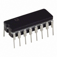
Package / Case
16-DIP
Number Of Elements
2
Output Type
Complementary, ECL, Open-Emitter
Mounting Type
Through Hole
Lead Free Status / RoHS Status
Contains lead / RoHS non-compliant
Available stocks
Company
Part Number
Manufacturer
Quantity
Price

Part Number:
AD96687BQ
Manufacturer:
ADI/亚德诺
Quantity:
20 000


AD96685/AD96687–SPECIFICATIONS
ELECTRICAL CHARACTERISTICS
Parameter
INPUT CHARACTERISTICS
ENABLE INPUT
DIGITAL OUTPUTS
SWITCHING PERFORMANCES
POWER SUPPLY
NOTES
1
2
3
4
5
6
7
Specifications subject to change without notice.
R
Input Voltage Range can be extended to –3.3 V if –V
Outputs terminated through 50 Ω to –2.0 V.
Propagation delays measured with 100 mV pulse (10 mV overdrive) to 50% transition point of the output.
Change in propagation delay from 100 mV to 1 V input overdrive.
Supply voltages should remain stable within ± 5% for normal operation.
Measured at ± 5% of +V
S
Input Offset Voltage
Input Offset Drift
Input Bias Current
Input Offset Current
Input Resistance
Input Capacitance
Input Voltage Ranges
Common-Mode Rejection Ratio
Logic “1” Voltage
Logic “0” Voltage
Logic “1” Current
Logic “0” Current
Logic “1” Voltage
Logic “0” Voltage
Propagation Delays
Dispersions
Latch Enable
Positive Supply Current (+5.0 V)
Negative Supply Current (–5.2 V)
Power Supply Rejection Ratio
= 100 Ω.
Input to Output HIGH
Input to Output LOW
Latch Enable to Output HIGH
Latch Enable to Output LOW
Minimum Pulsewidth
Minimum Setup Time
Minimum Hold Time
5
DIFFERENTIAL
6
S
VOLTAGE
ENABLE
and –V
4
3
LATCH
INPUT
2
S
Q
Q
.
COMPARE
LATCH
7
V
IN
S
V
Temp
25°C
Full
Full
25°C
Full
25°C
Full
25°C
25°C
Full
Full
Full
Full
Full
Full
Full
Full
25°C
25°C
25°C
25°C
25°C
25°C
25°C
25°C
Full
Full
Full
t
= –6.0 V.
DD
S
t
PD
t
H
(Positive Supply Voltage = 5.0 V; Negative Supply Voltage = –5.2 V, unless otherwise noted.)
Level
Test
VI
VI
VI
VI
VI
VI
VI
VI
VI
VI
VI
IV
IV
IV
IV
IV
IV
IV
VI
VI
VI
V
V
V
V
I
I
I
t
PW
t
PD
(E)
(E)
Min
–2.5
–1.1
–1.1
80
60
Industrial Temperature Range –25 C to +85 C
AD96685BR
50%
50%
50%
V
OS
Typ
1
20
7
0.1
200
2
2.5
2.5
2.5
2.5
50
2.0
0.5
0.5
70
90
8
15
Max
2
3
10
13
1.0
1.2
+5.0
–1.5
40
5
–1.5
3.5
3.5
3.5
3.5
3.0
1.0
1.0
9
18
t
t
t
t
t
V
V
PD
PD
PW
S
H
OS
OD
(E)
(E)
– Minimum Setup Time
– Minimum Hold Time
– Input to Output Delay
– LATCH ENABLE to Output Delay
– Minimum LATCH ENABLE Pulsewidth
– Input Offset Voltage
– Overdrive Voltage
Min
–2.5
80
–1.1
–1.1
60
AD96687BQ/BP/BR
Typ
1
20
7
0.1
200
2
90
2.5
2.5
2.5
2.5
50
2.0
0.5
0.5
15
31
70
Max
2
3
10
13
1.0
1.2
+5.0
–1.5
40
5
–1.5
3.5
3.5
3.5
3.5
3.0
1.0
1.0
18
36
Unit
mV
mV
µV/°C
µA
µA
µA
µA
kΩ
pF
V
dB
V
V
µA
µA
V
V
ns
ns
ns
ns
ps
ns
ns
ns
mA
mA
dB
Related parts for AD96687BQ
Image
Part Number
Description
Manufacturer
Datasheet
Request
R

Part Number:
Description:
±1.7g Dual-Axis IMEMS Accelerometer Evaluation Board
Manufacturer:
Analog Devices Inc
Datasheet:

Part Number:
Description:
Inertial Sensor Evaluation System
Manufacturer:
Analog Devices Inc
Datasheet:
Part Number:
Description:
Manufacturer:
Analog Devices Inc
Datasheet:
Part Number:
Description:
Manufacturer:
Analog Devices Inc
Datasheet:
Part Number:
Description:
Manufacturer:
Analog Devices Inc
Datasheet:
Part Number:
Description:
Manufacturer:
Analog Devices Inc
Datasheet:
Part Number:
Description:
Manufacturer:
Analog Devices Inc
Datasheet:
Part Number:
Description:
Manufacturer:
Analog Devices Inc
Datasheet:
Part Number:
Description:
Manufacturer:
Analog Devices Inc
Datasheet:
Part Number:
Description:
Manufacturer:
Analog Devices Inc
Datasheet:
Part Number:
Description:
Manufacturer:
Analog Devices Inc
Datasheet:
Part Number:
Description:
Manufacturer:
Analog Devices Inc
Datasheet:
Part Number:
Description:
Manufacturer:
Analog Devices Inc
Datasheet: