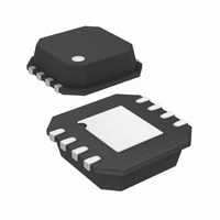
ADA4817-1ACPZ-R7 Analog Devices Inc, ADA4817-1ACPZ-R7 Datasheet - Page 13

ADA4817-1ACPZ-R7
Manufacturer Part Number
ADA4817-1ACPZ-R7
Description
Hi Speed FET Input Amp
Manufacturer
Analog Devices Inc
Series
FastFET™r
Datasheet
1.ADA4817-1ACPZ-R7.pdf
(24 pages)
Specifications of ADA4817-1ACPZ-R7
Amplifier Type
Voltage Feedback
Number Of Circuits
1
Slew Rate
870 V/µs
Gain Bandwidth Product
410MHz
-3db Bandwidth
1.05GHz
Current - Input Bias
2pA
Voltage - Input Offset
400µV
Current - Supply
19mA
Current - Output / Channel
40mA
Voltage - Supply, Single/dual (±)
5 V ~ 10 V, ±2.5 V ~ 5 V
Operating Temperature
-40°C ~ 105°C
Mounting Type
Surface Mount
Package / Case
8-LFCSP
Lead Free Status / RoHS Status
Lead free / RoHS Compliant
Output Type
-
Lead Free Status / RoHS Status
Lead free / RoHS Compliant
Other names
ADA4817-1ACPZ-R7TR
Available stocks
Company
Part Number
Manufacturer
Quantity
Price
Company:
Part Number:
ADA4817-1ACPZ-R7
Manufacturer:
Aptina
Quantity:
1 500
Part Number:
ADA4817-1ACPZ-R7
Manufacturer:
ADI/亚德诺
Quantity:
20 000
THEORY OF OPERATION
The ADA4817-1/ADA4817-2 are voltage feedback operational
amplifiers that combine new architecture for FET input opera-
tional amplifiers with the eXtra Fast Complementary Bipolar
(XFCB) process from Analog Devices resulting in an outstanding
combination of speed and low noise. The innovative high speed
FET input stage handles common-mode signals from the nega-
tive supply to within 2.3 V of the positive rail. This stage is
combined with an H-bridge to attain a 870 V/μs slew rate and
low distortion, in addition to 4 nV/√Hz input voltage noise.
The amplifier features a high speed output stage capable of driving
heavy loads sourcing and sinking up to 70 mA of linear current.
Supply current and offset current are laser trimmed for optimum
performance. These specifications make the ADA4817-1/
ADA4817-2 a great choice for high speed instrumentation
and high resolution data acquisition systems. Its low noise,
picoamp input current, precision offset, and high speed make
them superb preamps for fast photodiode applications.
CLOSED-LOOP FREQUENCY RESPONSE
The ADA4817-1/ADA4817-2 are classic voltage feedback
amplifiers with an open-loop frequency response that can be
approximated as the integrator response shown in Figure 40.
Basic closed-loop frequency response for inverting and nonin-
verting configurations can be derived from the schematics shown
in Figure 38 and Figure 39.
NONINVERTING CLOSED-LOOP FREQUENCY
RESPONSE
Solving for the transfer function,
where f
gain equals 0 dB.
At dc
V
V
V
V
O
I
CROSSOVER
O
I
=
=
(
R
R
F
F
R
+
2
is the frequency where the amplifier’s open-loop
Figure 38. Noninverting Configuration
+
G
π
V
R
Figure 39. Inverting Configuration
R
IN
×
G
G
)
f
S
R
CROSSOVER
V
G
+
IN
R
2
G
π
×
V
E
V
f
E
R
CROSSOVER
(
F
R
R
F
G
A
A
+
R
F
)
×
R
V
G
OUT
V
OUT
Rev. 0 | Page 13 of 24
(4)
(5)
Closed-loop −3 dB frequency
INVERTING CLOSED-LOOP FREQUENCY RESPONSE
Solving for the transfer function,
Solve for closed-loop −3 dB frequency by,
The closed-loop bandwidth is inversely proportional to the noise
gain of the op amp circuit, (R
accurate for noise gains above 2. The actual bandwidth of circuits
with noise gains at or below 2 is higher than those predicted
with this model due to the influence of other poles in the
frequency response of the real op amp.
Figure 41 shows a voltage feedback amplifier’s dc errors. For
both inverting and noninverting configurations,
V
OUT
80
60
40
20
0
At dc
V
Figure 40. Open-Loop Gain vs. Frequency and Basic Connections
f
V
f
(
−
−3
error
O
I
3dB
dB
=
0.1
=
=
(
V
V
Figure 41. Voltage Feedback Amplifier’s DC Errors
)
R
V
f
O
f
=
I
R
CROSSOVER
F
IN
CROSSOVER
G
I
=
+
b
+
−
−
R
A = (2π ×
×
2
G
R
R
R
π
S
R
)
G
F
S
×
S
1
×
+V
+
×
f
⎛
⎜
⎜
⎝
FREQUENCY (MHz)
R
2
OS
CROSSOVER
R
R
π
F
f
CROSSOVER
F
–
R
G
ADA4817-1/ADA4817-2
×
+
R
R
G
+
+
F
G
R
G
f
R
CROSSOVER
+ R
R
G
G
F
10
I
I
×
b
G
⎞
⎟
⎟
⎠
b
+
)/s
–
)/R
−
R
R
F
F
I
G
b
−
. This simple model is
A
×
×
R
R
G
100
F
+
f
CROSSOVER
V
OS
V
⎛
⎜
⎜
⎝
OUT
1000
R
G
= 410MHz
R
+
G
R
(10)
F
(6)
(7)
(8)
(9)
⎞
⎟
⎟
⎠


