ADA4817-1ACPZ-R7 Analog Devices Inc, ADA4817-1ACPZ-R7 Datasheet - Page 16
ADA4817-1ACPZ-R7
Manufacturer Part Number
ADA4817-1ACPZ-R7
Description
Hi Speed FET Input Amp
Manufacturer
Analog Devices Inc
Series
FastFET™r
Datasheet
1.ADA4817-1ACPZ-R7.pdf
(24 pages)
Specifications of ADA4817-1ACPZ-R7
Amplifier Type
Voltage Feedback
Number Of Circuits
1
Slew Rate
870 V/µs
Gain Bandwidth Product
410MHz
-3db Bandwidth
1.05GHz
Current - Input Bias
2pA
Voltage - Input Offset
400µV
Current - Supply
19mA
Current - Output / Channel
40mA
Voltage - Supply, Single/dual (±)
5 V ~ 10 V, ±2.5 V ~ 5 V
Operating Temperature
-40°C ~ 105°C
Mounting Type
Surface Mount
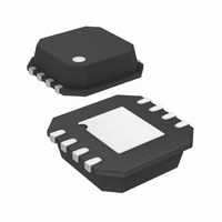
Package / Case
8-LFCSP
Lead Free Status / RoHS Status
Lead free / RoHS Compliant
Output Type
-
Lead Free Status / RoHS Status
Lead free / RoHS Compliant
Other names
ADA4817-1ACPZ-R7TR
Available stocks
Company
Part Number
Manufacturer
Quantity
Price
Company:

Part Number:
ADA4817-1ACPZ-R7
Manufacturer:
Aptina
Quantity:
1 500
Part Number:
ADA4817-1ACPZ-R7
Manufacturer:
ADI/亚德诺
Quantity:
20 000


ADA4817-1/ADA4817-2
LAYOUT, GROUNDING, AND BYPASSING CONSIDERATIONS
Laying out the PCB is usually the last step in the design process
and often proves to be one of the most critical. A brilliant
design can be rendered useless because of poor layout. Because
the ADA4817-1/ADA4817-2 can operate into the RF frequency
spectrum, high frequency board layout considerations must be
taken into account. The PCB layout, signal routing, power
supply bypassing, and grounding all must be addressed to
ensure optimal performance.
SIGNAL ROUTING
The ADA4817-1/ADA4817-2 feature the new low distortion
pinout with a dedicated feedback pin that allows a compact
layout. The dedicated feedback pin reduces the distance from
the output to the inverting input, which greatly simplifies the
routing of the feedback network.
When laying out the ADA4817-1/ADA4817-2 as a unity-gain
amplifier, it is recommended that a short, but wide, trace be
placed between the dedicated feedback pins, and the inverting
input to the amplifier be used to minimize stray parasitic
inductance.
To minimize parasitic inductances, ground planes should be
used under high frequency signal traces. However, the ground
plane should be removed from under the input and output pins
to minimize the formation of parasitic capacitors, which degrades
phase margin. Signals that are susceptible to noise pickup
should be run on the internal layers of the PCB, which can
provide maximum shielding.
POWER SUPPLY BYPASSING
Power supply bypassing is a critical aspect of the PCB design
process. For best performance, the ADA4817-1/ADA4817-2
power supply pins need to be properly bypassed.
A parallel connection of capacitors from each of the power
supply pins to ground works best. Paralleling different values
and sizes of capacitors helps to ensure that the power supply
pins see a low ac impedance across a wide band of frequencies.
This is important for minimizing the coupling of noise into the
amplifier. Starting directly at the power supply pins, the smallest
value and sized component should be placed on the same side
of the board as the amplifier, and as close as possible to the
amplifier, and connected to the ground plane. This process
should be repeated for the next larger value capacitor. It is
recommended that a 0.1 μF ceramic 0508 case be used for the
ADA4817-1/ADA4817-2. The 0508 offers low series inductance
and excellent high frequency performance. The 0.1 μF provides
low impedance at high frequencies. A 10 μF electrolytic capa-
citor should be placed in parallel with the 0.1 μF. The 10 μF
capacitor provides low ac impedance at low frequencies. Smaller
values of electrolytic capacitors may be used depending on the
circuit requirements. Additional smaller value capacitors help to
provide a low impedance path for unwanted noise out to higher
Rev. 0 | Page 16 of 24
frequencies but are not always necessary.
Placement of the capacitor returns (grounds) is also important.
Returning the capacitors grounds close to the amplifier load
is critical for distortion performance. Keeping the capacitors
distance short but equal from the load is optimal for performance.
In some cases, bypassing between the two supplies can help
to improve PSRR and to maintain distortion performance in
crowded or difficult layouts. It is another option to improve
performance.
Minimizing the trace length and widening the trace from the
capacitors to the amplifier reduces the trace inductance. A
series inductance with the parallel capacitance can form a
tank circuit, which can introduce high frequency ringing at
the output. This additional inductance can also contribute to
increased distortion due to high frequency compression at the
output. The use of vias should be minimized in the direct path
to the amplifier power supply pins because vias can introduce
parasitic inductance, which can lead to instability. When
required to use vias, choose multiple large diameter vias
because this lowers the equivalent parasitic inductance.
GROUNDING
The use of ground and power planes is encouraged as a method
of providing low impedance returns for power supply and signal
currents. Ground and power planes can also help to reduce stray
trace inductance and to provide a low thermal path for the
amplifier. Ground and power planes should not be used under
any of the pins. The mounting pads and the ground or power
planes can form a parasitic capacitance at the amplifier’s input.
Stray capacitance on the inverting input and the feedback
resistor form a pole, which degrades the phase margin, leading
to instability. Excessive stray capacitance on the output also
forms a pole, which degrades phase margin.
EXPOSED PADDLE
The ADA4817-1/ADA4817-2 feature an exposed paddle, which
lowers the thermal resistance by 25% compared to a standard
SOIC plastic package. The exposed paddle of the ADA4817-1/
ADA4817-2 floats internally which provides the maximum
flexibility and ease of use. It can be connected to the ground
plane or to the negative power supply plane. In cases where
thermal heating is not an issue, the exposed pad could be left
floating.
The use of thermal vias or heat pipes can also be incorporated
into the design of the mounting pad for the exposed paddle.
These additional vias help to lower the overall junction-to-
ambient temperature (θ
the surface to which the amplifier’s exposed paddle is soldered
can greatly reduce the overall thermal resistance seen by the
ADA4817-1/ADA4817-2.
JA
). Using a heavier weight copper on
Related parts for ADA4817-1ACPZ-R7
Image
Part Number
Description
Manufacturer
Datasheet
Request
R

Part Number:
Description:
IC OPAMP VF 410MHZ LN 40MA 8SOIC
Manufacturer:
Analog Devices Inc
Datasheet:

Part Number:
Description:
IC OPAMP VF 410MHZ LN 8LFCSP
Manufacturer:
Analog Devices Inc
Datasheet:
Part Number:
Description:
Hi Speed FET Input Amp
Manufacturer:
Analog Devices Inc
Datasheet:

Part Number:
Description:
High Speed FET Input Amp
Manufacturer:
Analog Devices Inc
Datasheet:
Part Number:
Description:
High Speed FET Input Amp
Manufacturer:
Analog Devices Inc
Datasheet:

Part Number:
Description:
Low Noise, 1 GHz FastFET Op Amps
Manufacturer:
Analog Devices
Datasheet:
Part Number:
Description:
Low Noise, 1 GHz FastFET Op Amps
Manufacturer:
Analog Devices
Datasheet:
Part Number:
Description:
Amplifier IC Development Tools ADA4817-1AR-EBZ_A00973_EB-O8REDF-1Z
Manufacturer:
Analog Devices
Datasheet:

Part Number:
Description:
Hi Speed FET Input Amp Dual
Manufacturer:
Analog Devices Inc
Datasheet:
Part Number:
Description:
ADA4817-1ACP-EBZ_A00975_EB-O8CP33-1Z
Manufacturer:
Analog Devices Inc
Part Number:
Description:
IC, OP-AMP, 1.05GHZ, 870V/µs, LFCSP-16
Manufacturer:
Analog Devices Inc
Datasheet:
Part Number:
Description:
Hi Speed FET Input Amp Dual
Manufacturer:
Analog Devices Inc
Datasheet:

Part Number:
Description:
±1.7g Dual-Axis IMEMS Accelerometer Evaluation Board
Manufacturer:
Analog Devices Inc
Datasheet:
Part Number:
Description:
Inertial Sensor Evaluation System
Manufacturer:
Analog Devices Inc
Datasheet:
Part Number:
Description:
Manufacturer:
Analog Devices Inc
Datasheet: