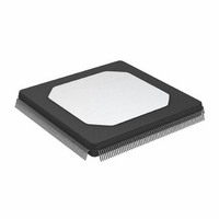
ADSP-21062LKS-133 Analog Devices Inc, ADSP-21062LKS-133 Datasheet - Page 32

ADSP-21062LKS-133
Manufacturer Part Number
ADSP-21062LKS-133
Description
Digital Signal Processor(DSP) IC
Manufacturer
Analog Devices Inc
Series
SHARC®r
Type
Floating Pointr
Specifications of ADSP-21062LKS-133
Rohs Status
RoHS non-compliant
Interface
Host Interface, Link Port, Serial Port
Clock Rate
33MHz
Non-volatile Memory
External
On-chip Ram
256kB
Voltage - I/o
3.30V
Voltage - Core
3.30V
Operating Temperature
0°C ~ 85°C
Mounting Type
Surface Mount
Package / Case
240-MQFP, 240-PQFP
Device Core Size
32b
Architecture
Super Harvard
Format
Floating Point
Clock Freq (max)
33MHz
Mips
33
Device Input Clock Speed
33MHz
Ram Size
256KB
Operating Supply Voltage (typ)
3.3V
Operating Supply Voltage (min)
3.15V
Operating Supply Voltage (max)
3.45V
Operating Temp Range
0C to 85C
Operating Temperature Classification
Commercial
Mounting
Surface Mount
Pin Count
240
Package Type
MQFP
Lead Free Status / Rohs Status
Not Compliant
Available stocks
Company
Part Number
Manufacturer
Quantity
Price
ADSP-21060/ADSP-21060L/ADSP-21062/ADSP-21062L/ADSP-21060C/ADSP-21060LC
Asynchronous Read/Write—Host to ADSP-2106x
Use these specifications for asynchronous host processor
accesses of an ADSP-2106x, after the host has asserted CS and
HBR (low). After HBG is returned by the ADSP-2106x, the host
can drive the RD and WR pins to access the ADSP-2106x’s
internal memory or IOP registers. HBR and HBG are assumed
low for this timing. Not required if and address are valid t
Table 19. Read Cycle
1
2
3
Table 20. Write Cycle
Parameter
Timing Requirements
t
t
t
t
t
Switching Characteristics
t
t
t
t
Parameter
Timing Requirements
t
t
t
t
t
t
t
t
t
Switching Characteristics
t
t
t
Not required if RD and address are valid t
For ADSP-21060L, specification is 10.5 ns max; for ADSP-21060LC, specification is 12.5 ns max.
For ADSP-21060L/ADSP-21060LC, specification is 2 ns min, 8.5 ns max.
SADRDL
HADRDH
WRWH
DRDHRDY
DRDHRDY
SDATRDY
DRDYRDL
RDYPRD
HDARWH
SCSWRL
HCSWRH
SADWRH
HADWRH
WWRL
WRWH
DWRHRDY
SDATWH
HDATWH
DRDYWRL
RDYPWR
SRDYCK
low or by t
ADSP-2106x” section in the ADSP-2106x SHARC User’s Manual, Revision 2.1.
HBGRCSV
after HBG goes low. This is easily accomplished by driving an upper address signal high when HBG is asserted. See the “Host Processor Control of the
Address Setup/CS Low Before RD Low
Address Hold/CS Hold Low After RD
RD/WR High Width
RD High Delay After REDY (O/D) Disable
RD High Delay After REDY (A/D) Disable
Data Valid Before REDY Disable from Low
REDY (O/D) or (A/D) Low Delay After RD Low
REDY (O/D) or (A/D) Low Pulse Width for Read
Data Disable After RD High
CS Low Setup Before WR Low
CS Low Hold After WR High
Address Setup Before WR High
Address Hold After WR High
WR Low Width
RD/WR High Width
WR High Delay After REDY (O/D) or (A/D) Disable
Data Setup Before WR High
Data Hold After WR High
REDY (O/D) or (A/D) Low Delay After WR/CS Low
REDY (O/D) or (A/D) Low Pulse Width for Write
REDY (O/D) or (A/D) Disable to CLKIN
HBGRCSV
after HBG goes low. For first access after HBR asserted, ADDR31-0 must be a non-MMS value 1/2 t
3
Rev. F | Page 32 of 64 | March 2008
HBGRCSV
1
2
after goes low. For first access after asserted, ADDR31–0 must
be a non-MMS value 1/2 t
after goes low. This is easily accomplished by driving an upper
address signal high when is asserted. See the “Host Processor
Control of the ADSP-2106x” section in the ADSP-2106x
SHARC User’s Manual, Revision 2.1.
Min
0
0
5
2
7
6
0
5
1
15 + 7DT/16
1 + 7DT/16
Min
0
0
6
0
0
2
45 + 21DT/16
2
CLK
5 V and 3.3 V
5 V and 3.3 V
before or goes low or by t
Max
10
8
Max
10
8 + 7DT/16
CLK
before RD or WR goes
HBGRCSV
Unit
ns
ns
ns
ns
ns
ns
ns
ns
ns
Unit
ns
ns
ns
ns
ns
ns
ns
ns
ns
ns
ns
ns


