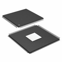
ADSP-21369BSWZ-2A Analog Devices Inc, ADSP-21369BSWZ-2A Datasheet - Page 35

ADSP-21369BSWZ-2A
Manufacturer Part Number
ADSP-21369BSWZ-2A
Description
333 MHz, Shared Memory,S/PDIF EPAD PBfr
Manufacturer
Analog Devices Inc
Series
SHARC®r
Type
Floating Pointr
Datasheet
1.ADSP-21369KBPZ-2A.pdf
(60 pages)
Specifications of ADSP-21369BSWZ-2A
Interface
DAI, DPI
Clock Rate
333MHz
Non-volatile Memory
ROM (768 kB)
On-chip Ram
256kB
Voltage - I/o
3.30V
Voltage - Core
1.20V
Operating Temperature
-40°C ~ 85°C
Mounting Type
Surface Mount
Package / Case
208-LQFP
Device Core Size
32/40Bit
Architecture
Super Harvard
Format
Floating Point
Clock Freq (max)
333MHz
Mips
333
Device Input Clock Speed
333MHz
Ram Size
256KB
Program Memory Size
768KB
Operating Supply Voltage (typ)
1.2/3.3V
Operating Supply Voltage (min)
1.14/3.13V
Operating Supply Voltage (max)
1.26/3.47V
Operating Temp Range
-40C to 85C
Operating Temperature Classification
Industrial
Mounting
Surface Mount
Pin Count
208
Package Type
LQFP EP
Package
208LQFP EP
Numeric And Arithmetic Format
Floating-Point
Maximum Speed
333 MHz
Device Million Instructions Per Second
333 MIPS
Lead Free Status / RoHS Status
Lead free / RoHS Compliant
Lead Free Status / RoHS Status
Lead free / RoHS Compliant
Available stocks
Company
Part Number
Manufacturer
Quantity
Price
Company:
Part Number:
ADSP-21369BSWZ-2A
Manufacturer:
Analog Devices Inc
Quantity:
10 000
Table 29. Serial Ports—Internal Clock
1
2
3
Table 30. Serial Ports—Enable and Three-State
1
Table 31. Serial Ports—External Late Frame Sync
1
Parameter
Timing Requirements
t
t
t
t
Switching Characteristics
t
t
t
t
t
t
t
Referenced to the sample edge.
Referenced to drive edge.
Minimum SPORT divisor register value.
Parameter
Switching Characteristics
t
t
t
Referenced to drive edge.
Parameter
Switching Characteristics
t
t
The t
SFSI
HFSI
SDRI
HDRI
DFSI
HOFSI
DFSIR
HOFSIR
DDTI
HDTI
SCLKIW
DDTEN
DDTTE
DDTIN
DDTLFSE
DDTENFS
1
1
2
1
2
1
2
2
2
1
1
1
2
DDTLFSE
3
1
1
and t
DDTENFS
parameters apply to left-justified sample pair as well as DSP serial mode, and MCE = 1, MFD = 0.
Data Enable from External Transmit SCLK
Data Disable from External Transmit SCLK
Data Enable from Internal Transmit SCLK
Data Delay from Late External Transmit FS or External Receive
FS with MCE = 1, MFD = 0
Data Enable for MCE = 1, MFD = 0
FS Setup Before SCLK
(Externally Generated FS in Either Transmit or Receive Mode)
FS Hold After SCLK
(Externally Generated FS in Either Transmit or Receive Mode)
Receive Data Setup Before SCLK
Receive Data Hold After SCLK
FS Delay After SCLK (Internally Generated FS in Transmit Mode)
FS Hold After SCLK (Internally Generated FS in Transmit Mode)
FS Delay After SCLK (Internally Generated FS in Receive Mode)
FS Hold After SCLK (Internally Generated FS in Receive Mode)
Transmit Data Delay After SCLK
Transmit Data Hold After SCLK
Transmit or Receive SCLK Width
Rev. E | Page 35 of 60 | July 2009
ADSP-21367/ADSP-21368/ADSP-21369
Min
2
–1
Min
0.5
Min
7
–1.0
–1.0
–1.0
2 × t
7
2.5
2.5
PCLK
– 1.5
Max
10
Max
7.75
Max
4
9.75
3.25
2 × t
PCLK
+ 1.5
Unit
ns
ns
ns
Unit
ns
ns
Unit
ns
ns
ns
ns
ns
ns
ns
ns
ns
ns
ns


