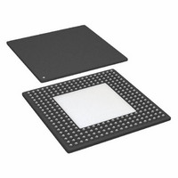
ADSP-21369KBPZ-3A Analog Devices Inc, ADSP-21369KBPZ-3A Datasheet - Page 50

ADSP-21369KBPZ-3A
Manufacturer Part Number
ADSP-21369KBPZ-3A
Description
IC,DSP,32-BIT,CMOS,BGA,256PIN,PLASTIC
Manufacturer
Analog Devices Inc
Series
SHARC®r
Type
Floating Pointr
Datasheet
1.ADSP-21369KBPZ-2A.pdf
(60 pages)
Specifications of ADSP-21369KBPZ-3A
Interface
DAI, DPI
Clock Rate
400MHz
Non-volatile Memory
ROM (768 kB)
On-chip Ram
256kB
Voltage - I/o
3.30V
Voltage - Core
1.20V
Operating Temperature
0°C ~ 70°C
Mounting Type
Surface Mount
Package / Case
256-BGA Exposed Pad, 256-eBGA, 256-HBGA
Lead Free Status / RoHS Status
Lead free / RoHS Compliant
For Use With
ADZS-21369-EZLITE - KIT EVAL EZ LITE ADDS-21369
Lead Free Status / RoHS Status
Lead free / RoHS Compliant
Available stocks
Company
Part Number
Manufacturer
Quantity
Price
Company:
Part Number:
ADSP-21369KBPZ-3A
Manufacturer:
TOREX
Quantity:
6 700
Company:
Part Number:
ADSP-21369KBPZ-3A
Manufacturer:
Analog Devices Inc
Quantity:
10 000
Part Number:
ADSP-21369KBPZ-3A
Manufacturer:
ADI/亚德诺
Quantity:
20 000
ADSP-21367/ADSP-21368/ADSP-21369
THERMAL CHARACTERISTICS
The ADSP-21367/ADSP-21368/ADSP-21369 processors are
rated for performance over the temperature range specified in
Operating Conditions on Page
Table 43
JEDEC standards JESD51-2 and JESD51-6 and the junction-to-
board measurement complies with JESD51-8. Test board design
complies with JEDEC standards JESD51-9 (BGA_ED) and
JESD51-8 (LQFP_EP). The junction-to-case measurement com-
plies with MIL-STD-883. All measurements use a 2S2P JEDEC
test board.
The LQFP-EP package requires thermal trace squares and ther-
mal vias, to an embedded ground plane, in the PCB. Refer to
JEDEC standard JESD51-5 for more information.
Figure 47. SDCLK Typical Output Delay or Hold vs. Load Capacitance
Figure 46. Typical Output Delay or Hold vs. Load Capacitance
- 2
- 2
- 4
10
8
6
4
0
2
8
6
4
2
0
and
0
0
Table 44
y = 0.0256x
(at Junction Temperature)
(at Junction Temperature)
50
airflow measurements comply with
50
y = 0.0488x - 1.5923
LOAD CAPACITANCE (pF)
-
LOAD CAPACITANCE (pF)
0.021
16.
100
100
150
150
Rev. E | Page 50 of 60 | July 2009
200
200
To determine the junction temperature of the device while on
the application PCB, use:
where:
T
T
package
the typical value from
P
Values of
design considerations.
mation of T
where:
T
Values of
design considerations when an external heat sink is required.
This is only applicable when a heat sink is used.
Values of
design considerations. The thermal characteristics values pro-
vided in
Table 43. Thermal Characteristics for 256-Ball BGA_ED
Table 44. Thermal Characteristics for 208-Lead LQFP EPAD
(With Exposed Pad Soldered to PCB)
Parameter
Parameter
D
J
TOP
A
JT
JA
JMA
JMA
JC
JB
JA
JMA
JMA
JC
T
T
= junction temperature ( C)
JT
JMT
JMT
JT
JMT
JMT
JB
JMB
JMB
= power dissipation (see EE Note EE-299)
= ambient temperature ( C)
= junction-to-top (of package) characterization parameter is
J
J
= case temperature ( C) measured at the top center of the
=
=
T
T
Table 43
A
TOP
JA
JC
JB
J
+
are provided for package comparison and PCB
are provided for package comparison and PCB
by the equation:
are provided for package comparison and PCB
+
Condition
Airflow = 0 m/s
Airflow = 1 m/s
Airflow = 2 m/s
Airflow = 0 m/s
Airflow = 1 m/s
Airflow = 2 m/s
Condition
Airflow = 0 m/s
Airflow = 1 m/s
Airflow = 2 m/s
Airflow = 0 m/s
Airflow = 1 m/s
Airflow = 2 m/s
Airflow = 0 m/s
Airflow = 1 m/s
Airflow = 2 m/s
JA
and
JT
P
Table 44
Table 43
D
JA
P
D
can be used for a first-order approxi-
are modeled values @ 2 W.
and
Table
44.
Typical
12.5
10.6
9.9
0.7
5.3
0.3
0.3
0.3
Typical
17.1
14.7
14.0
9.6
0.23
0.39
0.45
11.5
11.2
11.0
Unit
Unit
C/W
C/W
C/W
C/W
C/W
C/W
C/W
C/W
C/W
C/W
C/W
C/W
C/W
C/W
C/W
C/W
C/W
C/W


