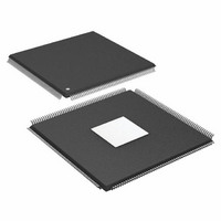
ADSP-21369KSWZ-1A Analog Devices Inc, ADSP-21369KSWZ-1A Datasheet - Page 30

ADSP-21369KSWZ-1A
Manufacturer Part Number
ADSP-21369KSWZ-1A
Description
266 MHz, Shared Memory,S/PDIF EPAD PBfr
Manufacturer
Analog Devices Inc
Series
SHARC®r
Type
Floating Pointr
Datasheet
1.ADSP-21369KBPZ-2A.pdf
(60 pages)
Specifications of ADSP-21369KSWZ-1A
Interface
DAI, DPI
Clock Rate
266MHz
Non-volatile Memory
ROM (768 kB)
On-chip Ram
256kB
Voltage - I/o
3.30V
Voltage - Core
1.20V
Operating Temperature
0°C ~ 70°C
Mounting Type
Surface Mount
Package / Case
208-LQFP
Device Core Size
32/40Bit
Architecture
Super Harvard
Format
Floating Point
Clock Freq (max)
266MHz
Mips
266
Device Input Clock Speed
266MHz
Ram Size
256KB
Program Memory Size
768KB
Operating Supply Voltage (typ)
1.2/3.3V
Operating Supply Voltage (min)
1.14/3.13V
Operating Supply Voltage (max)
1.26/3.47V
Operating Temp Range
0C to 70C
Operating Temperature Classification
Commercial
Mounting
Surface Mount
Pin Count
208
Package Type
LQFP EP
Lead Free Status / RoHS Status
Lead free / RoHS Compliant
For Use With
ADZS-21369-EZLITE - KIT EVAL EZ LITE ADDS-21369
Lead Free Status / Rohs Status
Compliant
Available stocks
Company
Part Number
Manufacturer
Quantity
Price
Company:
Part Number:
ADSP-21369KSWZ-1A
Manufacturer:
Analog Devices Inc
Quantity:
10 000
ADSP-21367/ADSP-21368/ADSP-21369
Memory Read
Use these specifications for asynchronous interfacing to memo-
ries. These specifications apply when the processors are the bus
master accessing external memory space in asynchronous access
mode. Note that timing for ACK, DATA, RD, WR, and strobe
timing parameters only apply to asynchronous access mode.
Table 24. Memory Read
1
2
3
4
Parameter
Timing Requirements
t
t
t
t
t
t
Switching Characteristics
t
t
t
t
W = (number of wait states specified in AMICTLx register) × t
HI =RHC + IC (RHC = number of read hold cycles specified in AMICTLx register) × t
IC = (number of idle cycles specified in AMICTLx register) × t
H = (number of hold cycles specified in AMICTLx register) × t
The falling edge of MSx is referenced.
Note that timing for ACK, DATA, RD, WR, and strobe timing parameters only apply to asynchronous access mode.
Data hold: User must meet t
ACK delay/setup: User must meet t
DAD
DRLD
SDS
HDRH
DAAK
DSAK
DRHA
DARL
RW
RWR
ADDR
DATA
MSx
ACK
WR
RD
Address, Selects Delay to Data Valid
RD Low to Data Valid
Data Setup to RD High
Data Hold from RD High
ACK Delay from Address, Selects
ACK Delay from RD Low
Address Selects Hold After RD High
Address Selects to RD Low
RD Pulse Width
RD High to WR, RD Low
HDA
or t
DAAK
HDRH
t
, or t
DARL
in asynchronous access mode. See
DSAK
t
DAAK
, for deassertion of ACK (low). For asynchronous assertion of ACK (high), user must meet t
4
2, 3
1
t
t
DSAK
DAD
1, 4
Rev. E | Page 30 of 60 | July 2009
1
t
DRLD
Figure 19. Memory Read
SDCLK
SDCLK
SDCLK
Test Conditions on Page 48
.
.
.
t
RW
Min
2.5
0
RH + 0.20
t
W – 1.4
HI + t
SDCLK
– 3.3
SDCLK
– 0.8
t
SDS
SDCLK
for the calculation of hold times given capacitive and dc loads.
Max
W + t
W – 3.2
t
W – 7.0
SDCLK
t
HDRH
–9.5 + W
t
SDCLK
DRHA
t
RWR
–5.12
DAAK
or t
DSAK
.
Unit
ns
ns
ns
ns
ns
ns
ns
ns
ns
ns


