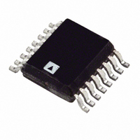
ADT7516ARQ Analog Devices Inc, ADT7516ARQ Datasheet - Page 34

ADT7516ARQ
Manufacturer Part Number
ADT7516ARQ
Description
DTS,12-Bit Quad DAC,4 Analog Inputs I.C.
Manufacturer
Analog Devices Inc
Datasheet
1.ADT7517ARQZ.pdf
(44 pages)
Specifications of ADT7516ARQ
Rohs Status
RoHS non-compliant
Function
Temp Monitoring System (Sensor)
Topology
ADC, Comparator, Multiplexer, Register Bank
Sensor Type
External & Internal
Sensing Temperature
-40°C ~ 120°C, External Sensor
Output Type
I²C™, MICROWIRE™, QSPI™, SPI™
Output Alarm
No
Output Fan
No
Voltage - Supply
2.7 V ~ 5.5 V
Operating Temperature
-40°C ~ 120°C
Mounting Type
Surface Mount
Package / Case
16-QSOP
Lead Free Status / RoHS Status
Contains lead / RoHS non-compliant
For Use With
EVAL-ADT7516EBZ - BOARD EVALUATION FOR ADT7516
Lead Free Status / RoHS Status
Contains lead / RoHS non-compliant
Available stocks
Company
Part Number
Manufacturer
Quantity
Price
Part Number:
ADT7516ARQZ
Manufacturer:
ADI/亚德诺
Quantity:
20 000
ADT7516/ADT7517/ADT7519
Table 21.
Bit
D0
D1
D2
D3
D4
D5
D6
D7
Interrupt Mask 2 Register (Read/Write) [Address = 0x1E]
This mask register is an 8-bit read/write register that can be
used to mask any interrupts that can cause the INT/ INT pin to
go active.
D7
D7
0
1
Table 22.
Bit
[D0:D3]
D4
[D5:D7]
Internal Temperature Offset Register (Read/Write)
[Address = 0x1F]
This register contains the offset value for the internal temperature
channel. A twos complement number can be written to this
register and then added to the measured result before it is stored
or compared to limits. In this way, a one-point calibration can
be done, whereby the whole transfer function of the channel
can be moved up or down. From a software point of view, this
can be a very simple method to vary the characteristics of the
measurement channel if the thermal characteristics change.
Because it is an 8-bit register, the temperature resolution is 1°C.
D7
D7
0
1
Default settings at power-up.
Default settings at power-up.
1
1
Function
0 = enable internal T
1 = disable internal T
0 = enable internal T
1 = disable internal T
0 = enable external T
1 = disable external T
0 = enable external T
1 = disable external T
0 = enable external temperature fault interrupt.
1 = disable external temperature fault interrupt.
0 = enable AIN2 interrupt.
1 = disable AIN2 interrupt.
0 = enable AIN3 interrupt.
1 = disable AIN3 interrupt.
0 = enable AIN4 interrupt.
1 = disable AIN4 interrupt.
D6
D6
0
D6
D6
0
1
1
Reserved. Write 0s only.
Reserved. Write 0s only.
Function
0 = enable V
1 = disable V
D5
D5
0
D5
D5
0
1
1
D4
D4
0
D4
D4
0
HIGH
LOW
HIGH
LOW
1
1
HIGH
LOW
HIGH
LOW
DD
DD
interrupt.
interrupts.
interrupt.
interrupt.
interrupt.
interrupt.
interrupts.
interrupt.
interrupt or AIN1 interrupt.
interrupt or AIN1 interrupt.
D3
D3
0
D3
D3
0
1
1
D2
D2
0
D2
D2
0
1
1
D1
D1
0
D1
D1
0
1
1
D0
D0
0
D0
D0
0
1
1
Rev. B | Page 34 of 44
External Temperature Offset Register (Read/Write)
[Address = 0x20]
This register contains the offset value for the external temperature
channel. A twos complement number can be written to this
register and is then added to the measured result before it is
stored or compared to limits. In this way, a one-point calibration
can be done, whereby the whole transfer function of the channel
can be moved up or down. From a software point of view, this
can be a very simple method to vary the characteristics of the
measurement channel if the thermal characteristics change.
Because it is an 8-bit register, the temperature resolution is 1°C.
D7
D7
0
1
Internal Analog Temperature Offset Register
(Read/Write) [Address = 0x21]
This register contains the offset value for the internal thermal
voltage output. A twos complement number can be written to
this register and then added to the measured result before it is
converted by DAC A. Varying the value in this register has the
effect of varying the temperature span. For example, the output
voltage can represent a temperature span of −128°C to +127°C
or even 0°C to +127°C. In essence, this register changes the
position of 0 V on the temperature scale. Temperatures other
than −128°C to +127°C produce an upper deadband on the
DAC A output. Because it is an 8-bit register, the temperature
resolution is 1°C. The default value is −40°C.
D7
D7
1
1
External Analog Temperature Offset Register
(Read/Write) [Address = 0x22]
This register contains the offset value for the external thermal
voltage output. A twos complement number can be written to
this register and then added to the measured result before it is
converted by DAC B. Varying the value in this register has the
effect of varying the temperature span. For example, the output
voltage can represent a temperature span of −128°C to +127°C
or even 0°C to +127°C. In essence, this register changes the
position of 0 V on the temperature scale. Temperatures other
than −128°C to +127°C produce an upper deadband on the
DAC B output. Because it is an 8-bit register, the temperature
resolution is 1°C. The default value is −40°C.
D7
D7
1
1
Default settings at power-up.
Default settings at power-up.
Default settings at power-up.
1
1
1
D6
D6
0
D6
D6
1
D6
D6
1
1
1
1
D5
D5
0
D5
D5
0
D5
D5
0
1
1
1
D4
D4
0
D4
D4
1
D4
D4
1
1
1
1
D3
D3
0
D3
D3
1
D3
D3
1
1
1
1
D2
D2
0
D2
D2
0
D2
D2
0
1
1
1
D1
D1
0
D1
D1
0
D1
D1
0
1
1
1
D0
D0
0
D0
D0
0
D0
D0
0
1
1
1


