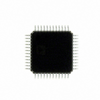
ADUC7060BSTZ32 Analog Devices Inc, ADUC7060BSTZ32 Datasheet - Page 26

ADUC7060BSTZ32
Manufacturer Part Number
ADUC7060BSTZ32
Description
DUAL 24-BIT AFE AND ARM 7 I.C
Manufacturer
Analog Devices Inc
Series
MicroConverter® ADuC7xxxr
Specifications of ADUC7060BSTZ32
Design Resources
4 mA-to-20 mA Loop-Powered Temperature Monitor Using ADuC7060/1 (CN0145) Low power, Long Range, ISM Wireless Measuring Node (CN0164)
Core Processor
ARM7
Core Size
16/32-Bit
Speed
10MHz
Connectivity
I²C, SPI, UART/USART
Peripherals
POR, PWM, Temp Sensor, WDT
Number Of I /o
14
Program Memory Size
32KB (16K x 16)
Program Memory Type
FLASH
Ram Size
4K x 8
Voltage - Supply (vcc/vdd)
2.375 V ~ 2.625 V
Data Converters
A/D 5x24b, 8x24b, D/A 1x14b
Oscillator Type
Internal
Operating Temperature
-40°C ~ 125°C
Package / Case
48-LQFP
Cpu Family
ADuC7xxx
Device Core
ARM7TDMI
Device Core Size
16/32Bit
Frequency (max)
10.24MHz
Interface Type
I2C/SPI/UART
Total Internal Ram Size
4KB
# I/os (max)
14
Number Of Timers - General Purpose
4
Operating Supply Voltage (typ)
2.5V
Operating Supply Voltage (max)
2.625V
Operating Supply Voltage (min)
2.375V
On-chip Adc
2(4-chx24-bit)
Instruction Set Architecture
RISC
Operating Temp Range
-40C to 125C
Operating Temperature Classification
Automotive
Mounting
Surface Mount
Pin Count
48
Package Type
LQFP
Package
48LQFP
Family Name
ADuC7xxx
Maximum Speed
10.24 MHz
Operating Supply Voltage
2.5 V
Data Bus Width
16|32 Bit
Number Of Programmable I/os
14
Number Of Timers
4
Lead Free Status / RoHS Status
Lead free / RoHS Compliant
Eeprom Size
-
Lead Free Status / Rohs Status
Compliant
Available stocks
Company
Part Number
Manufacturer
Quantity
Price
Company:
Part Number:
ADUC7060BSTZ32
Manufacturer:
CYPRESS
Quantity:
294
Company:
Part Number:
ADUC7060BSTZ32
Manufacturer:
ADI
Quantity:
315
Company:
Part Number:
ADUC7060BSTZ32
Manufacturer:
Analog Devices Inc
Quantity:
10 000
Part Number:
ADUC7060BSTZ32
Manufacturer:
ADI/亚德诺
Quantity:
20 000
Company:
Part Number:
ADUC7060BSTZ32-RL
Manufacturer:
Analog Devices Inc
Quantity:
10 000
ADuC7060/ADuC7061
MEMORY MAPPED REGISTERS
The memory mapped register (MMR) space is mapped into the
upper two pages of the memory array and is accessed by
indirect addressing through the ARM7 banked registers.
The MMR space provides an interface between the CPU and all
on-chip peripherals. All registers, except the core registers, reside
in the MMR area. All shaded locations shown in Figure 12 are
unoccupied or reserved locations and should not be accessed by
user software. Figure 12 shows the full MMR memory map.
The access time for reading from or writing to an MMR
depends on the advanced microcontroller bus architecture
(AMBA) bus used to access the peripheral. The processor has
two AMBA buses: the advanced high performance bus (AHB)
used for system modules and the advanced peripheral bus
(APB) used for a lower performance peripheral. Access to the
AHB is one cycle, and access to the APB is two cycles. All
peripherals on the ADuC706x are on the APB except for the
Flash/EE memory, the GPIOs, and the PWM.
Rev. B | Page 26 of 108
0xFFFFFFFF
0xFFFF0FC0
0xFFFF0D50
0xFFFF0D00
0xFFFF0A14
0xFFFF0A00
0xFFFF048C
0xFFFF0F80
0xFFFF0E24
0xFFFF0E00
0xFFFF0948
0xFFFF0900
0xFFFF0730
0xFFFF0700
0xFFFF0620
0xFFFF0600
0xFFFF0570
0xFFFF0500
0xFFFF0490
0xFFFF0470
0xFFFF0450
0xFFFF0420
0xFFFF0404
0xFFFF0394
0xFFFF0380
0xFFFF0370
0xFFFF0360
0xFFFF0350
0xFFFF0340
0xFFFF0334
0xFFFF0320
0xFFFF0238
0xFFFF0220
0xFFFF0140
0xFFFF0000
Figure 12. Memory Mapped Registers
PLL AND OSCILLATOR
GENERAL-PURPOSE
GENERAL-PURPOSE
SYSTEM CONTROL
FLASH CONTROL
CONTROLLER
REFERENCE
WATCHDOG
REMAP AND
INTERFACE
SELECTION
INTERRUPT
BAND GAP
CONTROL
WAKE-UP
SPI/I
TIMER
TIMER
TIMER
TIMER
UART
PWM
GPIO
DAC
ADC
SPI
I
2
C
2
C


