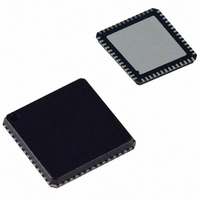
ADUC842BCPZ32-5 Analog Devices Inc, ADUC842BCPZ32-5 Datasheet - Page 18

ADUC842BCPZ32-5
Manufacturer Part Number
ADUC842BCPZ32-5
Description
Microconverter 1-cycle Version ADUC832
Manufacturer
Analog Devices Inc
Series
MicroConverter® ADuC8xxr
Specifications of ADUC842BCPZ32-5
Core Processor
8052
Core Size
8-Bit
Speed
16.78MHz
Connectivity
I²C, SPI, UART/USART
Peripherals
DMA, PSM, PWM, Temp Sensor, WDT
Number Of I /o
32
Program Memory Size
32KB (32K x 8)
Program Memory Type
FLASH
Ram Size
2.25K x 8
Voltage - Supply (vcc/vdd)
4.75 V ~ 5.25 V
Data Converters
A/D 8x12b, D/A 2x12b
Oscillator Type
Internal
Operating Temperature
-40°C ~ 85°C
Package / Case
56-LFCSP
Lead Free Status / RoHS Status
Lead free / RoHS Compliant
Eeprom Size
-
Lead Free Status / RoHS Status
Lead free / RoHS Compliant
Available stocks
Company
Part Number
Manufacturer
Quantity
Price
Company:
Part Number:
ADUC842BCPZ32-5
Manufacturer:
Analog Devices Inc
Quantity:
135
ADuC841/ADuC842/ADuC843
Mnemonic
Branching
Miscellaneous
1. One cycle is one clock.
2. Cycles of MOVX instructions are four cycles when they have 0 wait state. Cycles of MOVX instructions are 4 + n cycles when they have n wait states.
3. Cycles of LCALL instruction are three cycles when the LCALL instruction comes from interrupt.
OTHER SINGLE-CYCLE CORE FEATURES
Timer Operation
Timers on a standard 8052 increment by 1 with each machine
cycle. On the ADuC841/ADuC842/ADuC843, one machine
cycle is equal to one clock cycle; therefore the timers increment
at the same rate as the core clock.
ALE
The output on the ALE pin on a standard 8052 part is a clock at
1/6th of the core operating frequency. On the ADuC841/
ADuC842/ADuC843 the ALE pin operates as follows. For a
single machine cycle instruction,ALE is high for the first half of
the machine cycle and low for the second half. The ALE output
is at the core operating frequency. For a two or more machine
cycle instruction, ALE is high for the first half of the first
machine cycle and low for the rest of the machine cycles.
JMP @A+DPTR
RET
RETI
ACALL addr11
AJMP addr11
SJMP rel
JC rel
JNC rel
JZ rel
JNZ rel
DJNZ Rn,rel
LJMP
LCALL addr16
JB bit,rel
JNB bit,rel
JBC bit,rel
CJNE A,dir,rel
CJNE A,#data,rel
CJNE Rn,#data,rel
CJNE @Ri,#data,rel
DJNZ dir,rel
NOP
Description
Return from subroutine
Return from interrupt
Absolute jump to subroutine
Absolute jump unconditional
Long jump unconditional
Long jump to subroutine
Compare A, immediate JNE relative
Compare register, immediate JNE relative
Compare indirect, immediate JNE relative
Jump indirect relative to DPTR
Short jump (relative address)
Jump on carry equal to 1
Jump on carry equal to 0
Jump on accumulator = 0
Jump on accumulator not equal to 0
Decrement register, JNZ relative
Jump on direct bit = 1
Jump on direct bit = 0
Jump on direct bit = 1 and clear
Compare A, direct JNE relative
Decrement direct byte, JNZ relative
No operation
Rev. 0 | Page 18 of 88
External Memory Access
There is no support for external program memory access on the
parts. When accessing external RAM, the EWAIT register may
need to be programmed to give extra machine cycles to MOVX
commands. This is to account for differing external RAM access
speeds.
EWAIT SFR
SFR Address
Power-On Default
Bit Addressable
This special function register (SFR) is programmed with the
number of wait states for a MOVX instruction. This value can
range from 0H to 7H.
Bytes
1
1
1
2
2
2
2
2
2
2
2
3
3
3
3
3
3
3
3
3
3
1
9FH
00H
No
Cycles
3
4
4
3
3
3
3
3
3
3
3
4
4
4
4
4
4
4
4
4
4
1


