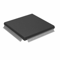
ADV611JSTZ Analog Devices Inc, ADV611JSTZ Datasheet - Page 19

ADV611JSTZ
Manufacturer Part Number
ADV611JSTZ
Description
CCTV Digital Video Codec
Manufacturer
Analog Devices Inc
Type
Video Codecr
Datasheet
1.ADV611JSTZ.pdf
(46 pages)
Specifications of ADV611JSTZ
Data Interface
Serial
Resolution (bits)
8 b
Sigma Delta
No
Voltage - Supply, Digital
4.5 V ~ 5.5 V
Operating Temperature
0°C ~ 70°C
Mounting Type
Surface Mount
Package / Case
120-LQFP
Lead Free Status / RoHS Status
Lead free / RoHS Compliant
Available stocks
Company
Part Number
Manufacturer
Quantity
Price
Company:
Part Number:
ADV611JSTZ
Manufacturer:
ADI
Quantity:
526
Company:
Part Number:
ADV611JSTZ
Manufacturer:
Analog Devices Inc
Quantity:
10 000
Part Number:
ADV611JSTZ
Manufacturer:
ADI
Quantity:
20 000
DRAM Interface Pins
Name
DDAT[15:0]
DADR[8:0]
RAS
CAS
WE
Host Interface Pins
Name
DATA[31:0]
ADR[1:0]
BE0–BE1
BE2–BE3
CS
WR
RD
REV. 0
Pins
16
9
1
1
1
Pins
32
2
2
1
1
1
I/O
O
I/O
O
O
O
I/O
I/O
I
I
I
I
I
Description
DRAM Data Bus. The ADV611/ADV612 uses these pins for 16-bit data read/
write operations to the external 256K 16-bit DRAM. (The operation of the
DRAM interface is fully automatic and controlled by internal functionality
of the ADV611/ADV612.) These pins are compatible with 30 pF loads.
DRAM Address Bus. The ADV611/ADV612 uses these pins to form the multi-
plexed row/column address lines to the external DRAM. (The operation of the
DRAM interface is fully automatic and controlled by internal functionality
of the ADV611/ADV612.) These pins are compatible with 30 pF loads.
DRAM Row Address Strobe. This pin is compatible with 30 pF loads.
DRAM Column Address Strobe. This pin is compatible with 30 pF loads.
DRAM Write Enable. This pin is compatible with 30 pF loads.
Note that the ADV611/ADV612 does not have a DRAM OE pin. Tie the
DRAM’s OE pin to ground.
Description
Host Data Bus. These pins make up a 32-bit wide host data bus. The host
controls this asynchronous bus with the WR, RD, BE and CS pins to commu-
nicate with the ADV611/ADV612. These pins are compatible with 30 pF loads.
Host DWord Address Bus. These two address pins let you address the
ADV611/ADV612’s four directly addressable host interface registers. For an
illustration of how this addressing works, see the Control and Write Register
Map figure and Status and Read Register Map figure. The ADR bits permit
register addressing as follows:
ADR1
0
0
1
1
Host Word Enable pins. These two input pins select the words that the ADV611/
ADV612’s direct and indirect registers access through the Host Interface;
BE0–BE1 access the least significant word, and BE2–BE3 access the most
significant word. For a 32-bit interface only, tie these pins to ground, making
all words available.
Some important notes for 16-bit interfaces are as follows:
• When using these byte enable pins, the byte order is always the lowest byte
•
• The ADV611/ADV612 advances to the next 32-bit compressed data FIFO
•
•
•
• The ADV611/ADV612 advances to the next 16-bit indirect register after the
•
•
Host Chip Select. This pin operates as follows:
• LO Qualifies Host Interface control signals
• HI Three-states DATA[31:0] pins
Host Write. Host register writes occur on the rising edge of this signal.
Host Read. Host register reads occur on the low true level of this signal.
to the higher bytes.
location after the BE2–BE3 pin is asserted then de-asserted (when accessing the
Compressed Data register); so the FIFO location only advances when and if
the host reads or writes the MSW of a FIFO location.
BE0–BE1 pin is asserted then de-asserted; so the register selection only advances
when and if the host reads or writes the MSW of a 16-bit indirect register.
ADR0
0
1
0
1
–19–
DWord
0
1
2
3
Address Byte Address
0x00
0x04
0x08
0x0C
ADV611/ADV612


