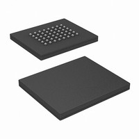
CY62167DV30LL-70BVIT Cypress Semiconductor Corp, CY62167DV30LL-70BVIT Datasheet - Page 8

CY62167DV30LL-70BVIT
Manufacturer Part Number
CY62167DV30LL-70BVIT
Description
CY62167DV30LL-70BVIT
Manufacturer
Cypress Semiconductor Corp
Datasheet
1.CY62167DV30LL-55ZXI.pdf
(17 pages)
Specifications of CY62167DV30LL-70BVIT
Format - Memory
RAM
Memory Type
SRAM
Memory Size
16M (2M x 8 or 1M x 16)
Speed
70ns
Interface
Parallel
Voltage - Supply
2.2 V ~ 3.6 V
Operating Temperature
-40°C ~ 85°C
Package / Case
48-VFBGA
Lead Free Status / RoHS Status
Contains lead / RoHS non-compliant
Available stocks
Company
Part Number
Manufacturer
Quantity
Price
Company:
Part Number:
CY62167DV30LL-70BVIT
Manufacturer:
Cypress Semiconductor Corp
Quantity:
10 000
Switching Waveforms
Notes
Document Number : 38-05328 Rev. *I
22. The internal Write time of the memory is defined by the overlap of WE, CE
23. Data I/O is high-impedance if OE = V
24. If CE
25. During this period, the I/Os are in output state and input signals should not be applied.
ADDRESS
BHE/BLE
a write and any of these signals can terminate a write by going INACTIVE. The data input set-up and hold timing should be referenced to the edge of the signal
that terminates the Write.
DATA I/O
1
goes HIGH and CE
CE
CE
WE
OE
2
1
See Note 25
2
goes LOW simultaneously with WE = V
(continued)
IH
.
t
SA
t
HZOE
Figure 4. Write Cycle 1 (WE Controlled)
t
AW
IH
, the output remains in a high-impedance state.
t
SCE
1
= V
t
WC
IL
, BHE and/or BLE = V
t
BW
VALID DATA
t
t
PWE
SD
[22, 23, 24]
IL
, and CE
2
= V
CY62167DV30 MoBL
IH
. All signals must be ACTIVE to initiate
t
HA
t
HD
Page 8 of 17


