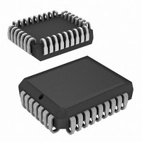
CY7B991V-5JXIT Cypress Semiconductor Corp, CY7B991V-5JXIT Datasheet - Page 10

CY7B991V-5JXIT
Manufacturer Part Number
CY7B991V-5JXIT
Description
IC,Eight Distributed-Output Clock Driver,LDCC,32PIN,PLASTIC
Manufacturer
Cypress Semiconductor Corp
Series
RoboClock™r
Type
Buffer/Driverr
Datasheet
1.CY7B991V-7JXC.pdf
(17 pages)
Specifications of CY7B991V-5JXIT
Number Of Circuits
1
Ratio - Input:output
8:8
Differential - Input:output
Yes/Yes
Input
3-State
Output
LVTTL
Frequency - Max
80MHz
Voltage - Supply
2.97 V ~ 3.63 V
Operating Temperature
-40°C ~ 85°C
Mounting Type
Surface Mount
Package / Case
32-PLCC
Frequency-max
80MHz
Lead Free Status / RoHS Status
Lead free / RoHS Compliant
Available stocks
Company
Part Number
Manufacturer
Quantity
Price
Company:
Part Number:
CY7B991V-5JXIT
Manufacturer:
Cypress Semiconductor Corp
Quantity:
10 000
Part Number:
CY7B991V-5JXIT
Manufacturer:
CYPRESS/赛普拉斯
Quantity:
20 000
Capacitance
Tested initially and after any design or process changes that may affect these parameters.
Switching Characteristics
Over the Operating Range
Document Number: 38-07141 Rev. *G
Note
C
f
t
t
t
t
t
t
t
t
t
t
t
t
t
t
t
t
t
t
NOM
RPWH
RPWL
U
SKEWPR
SKEW0
SKEW1
SKEW2
SKEW3
SKEW4
DEV
PD
ODCV
PWH
PWL
ORISE
OFALL
LOCK
JR
9. Applies to REF and FB inputs only. Tested initially and after any design or process changes that may affect these parameters.
IN
Parameter
Parameter
C
L
TTL AC Test Load
Operating clock
Frequency in MHz
REF pulse width HIGH
REF pulse width LOW
Programmable skew unit
Zero output matched-pair skew (XQ0, XQ1)
Zero output skew (all outputs)
Output skew (rise-rise, fall-fall, same class outputs)
Output skew (rise-fall, nominal-inverted, divided-divided)
Output skew (rise-rise, fall-fall, different class outputs)
Output skew (rise-fall, nominal-divided, divided-inverted)
Device-to-device skew
Propagation delay, REF rise to FB rise
Output duty cycle variation
Output HIGH time deviation from 50%
Output LOW time deviation from 50%
Output rise time
Output fall time
PLL lock time
Cycle-to-cycle output jitter
Input capacitance
V
CC
R1
R2
Description
R1=100
R2=100
C
(Includes fixture and probe capacitance)
[2, 10]
L
[21]
= 30 pF
[19, 20]
[19, 20]
[11, 17]
Figure 10. AC Test Loads and Waveforms
[18]
Description
[12, 14]
T
A
= 25 °C, f = 1 MHz, V
[19]
[19]
FS = LOW
FS = MID
FS = HIGH
RMS
Peak
[12, 13]
[11]
[11]
Test Conditions
[1, 2]
[1, 2]
[1, 2 , 3]
[12, 16]
[12, 16]
[12, 16]
[12, 16]
CC
V
th
= 3.3 V
=1.5 V
0.0 V
≤ 1 ns
0.8 V
2.0 V
TTL Input Test Waveform
–0.25
–0.65
0.15
0.15
Min
5.0
5.0
15
25
40
–
–
–
–
–
–
–
–
–
–
–
–
[9]]
3.0 V
CY7B991V–2
Max
0.05
0.25
10
Typ
100
0.1
0.1
0.5
0.5
0.0
0.0
1.0
1.0
See
–
–
–
–
–
–
–
–
–
–
Table 2
2.0 V
V
0.8 V
≤ 1 ns
th
+0.25
+0.65
0.25
Max
1.25
200
=1.5 V
0.2
0.5
1.0
0.5
0.9
2.0
1.5
1.2
1.2
0.5
30
50
80
25
–
–
CY7B991V
Unit
pF
Page 10 of 17
MHz
Unit
ms
ns
ns
ns
ns
ns
ns
ns
ns
ns
ns
ns
ns
ns
ns
ns
ps
ps
[+] Feedback


