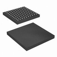
CY7B994V-5BBC Cypress Semiconductor Corp, CY7B994V-5BBC Datasheet - Page 11

CY7B994V-5BBC
Manufacturer Part Number
CY7B994V-5BBC
Description
IC,Sixteen Distributed-Output Clock Driver,BGA,100PIN,PLASTIC
Manufacturer
Cypress Semiconductor Corp
Series
RoboClock™r
Type
Clock Buffer, Fanout Distributionr
Datasheet
1.CY7B993V-2AXC.pdf
(18 pages)
Specifications of CY7B994V-5BBC
Pll
Yes
Input
LVPECL, LVTTL
Output
LVTTL
Number Of Circuits
1
Ratio - Input:output
4:18
Differential - Input:output
No/No
Frequency - Max
200MHz
Divider/multiplier
Yes/Yes
Voltage - Supply
2.97 V ~ 3.63 V
Operating Temperature
0°C ~ 70°C
Mounting Type
Surface Mount
Package / Case
100-LBGA
Frequency-max
200MHz
Lead Free Status / RoHS Status
Contains lead / RoHS non-compliant
Available stocks
Company
Part Number
Manufacturer
Quantity
Price
Company:
Part Number:
CY7B994V-5BBC
Manufacturer:
CY
Quantity:
2 286
Company:
Part Number:
CY7B994V-5BBC
Manufacturer:
CYPRESS
Quantity:
219
Company:
Part Number:
CY7B994V-5BBC
Manufacturer:
Cypress Semiconductor Corp
Quantity:
10 000
Company:
Part Number:
CY7B994V-5BBCT
Manufacturer:
CYPRESS
Quantity:
213
Company:
Part Number:
CY7B994V-5BBCT
Manufacturer:
Cypress Semiconductor Corp
Quantity:
10 000
Electrical Characteristics
Capacitance
Switching Characteristics
Document #: 38-07127 Rev. *I
Operating Current
I
I
C
f
f
t
t
t
t
t
t
t
t
t
t
Notes
Parameter
CCI
CCN
IN
OUT
SKEWPR
SKEWBNK
SKEW0
SKEW1
SKEW2
SKEW3
SKEWCPR
CCJ1-3
CCJ4-12
PD
7. I
8. This is dependent upon frequency and number of outputs of a bank being loaded. The value indicates maximum I
9. This is for non-three level inputs.
10. Assumes 25 pF Max load capacitance up to 185 MHz. At 200 MHz the Max load is 10 pF.
11. Both outputs of pair must be terminated, even if only one is being used.
12. Each package must be properly decoupled.
13. AC parameters are measured at 1.5V unless otherwise indicated.
14. Test Load C
15. SKEW is defined as the time between the earliest and the latest output transition among all outputs for which the same phase delay has been selected when
16. Complementary output skews are measured at complementary signal pair intersections.
17. Guaranteed by statistical correlation. Tested initially and after any design or process changes that may affect these parameters.
Parameter
Parameter
IN
CY7B994V), and all other clock output banks to run at half the maximum frequency. FS and OUTPUT_MODE are asserted to the HIGH state.
load of 25 pF terminated to 50 at V
all outputs are loaded with 25 pF and properly terminated up to 185 MHz. At 200 MHz the max load is 10 pF.
CCI
measurement is performed with Bank1 and FB Bank configured to run at maximum frequency (f
L
Clock Input Frequency
Clock Output Frequency
Matched-Pair Skew
Intrabank Skew
Output-Output Skew (same frequency and phase, rise to
rise, fall to fall)
Output-Output Skew (same frequency and phase, other
banks at different frequency, rise to rise, fall to fall)
Output-Output Skew (invert to nominal of different banks,
compared banks at same frequency, rising edge to falling
edge aligned, other banks at same frequency)
Output-Output Skew (all output configurations outside of
t
Complementary Outputs Skew (crossing to crossing,
complementary outputs of the same bank)
Cycle-to-Cycle Jitter (divide by 1 output frequency,
FB = divide by 1, 2, 3)
Cycle-to-Cycle Jitter (divide by 1 output frequency,
FB = divide by 4, 5, 6, 8, 10, 12)
Propagation Delay, REF to FB Rise
= 25 pF, terminated to V
SKEW1
Internal Operating
Current
Output Current
Dissipation/Pair
Input Capacitance
Description
and t
SKEW2
Description
[14, 15]
[14, 15]
[8]
)
CC
[14, 15]
CC
[14, 15]
/2.
/2 with 50up to185 MHz and 10 pF load to 200 MHz.
Over the Operating Range (continued)
CY7B993V
CY7B994V
CY7B993V
CY7B994V
Description
Over the Operating Range
T
[14, 15, 16, 17]
A
= 25
[14, 15]
CY7B993V
CY7B994V
CY7B993V
CY7B994V
C, f = 1 MHz, V
[14, 15]
[9, 10, 11, 12, 13]
Test Conditions
V
V
C
R
f
MAX
CC
CC
LOAD
LOAD
–250
Min
12
24
12
24
–
–
–
–
–
–
–
–
–
CY7B993/4V-2
Test Conditions
= Max, f
= Max,
CC
= 25 pF,
= 50 at V
NOM
Typ
= 3.3V
50
50
–
–
–
–
–
–
–
–
–
–
–
–
MAX
= 100 MHz for CY7B993V, f
Max
[7]
100
200
100
200
200
200
250
250
250
500
200
150
100
250
CC
CCN
/2,
CY7B993V, CY7B994V
at maximum frequency and maximum
–500
Min
12
24
12
24
Min
–
–
–
–
–
–
–
–
–
CY7B993/4V-5
–
Min
–
–
–
–
Typ
50
50
–
–
–
–
–
–
–
–
–
–
–
–
NOM
Max
RoboClock
= 200 MHz for
Max
5
100
200
100
200
200
250
550
650
700
800
300
150 ps Peak
100 ps Peak
500
Max
250
250
40
50
Page 11 of 18
Unit
MHz
MHz
MHz
MHz
Unit
ps
ps
ps
ps
ps
ps
ps
ps
pF
Unit
mA
mA
mA
mA
[+] Feedback


