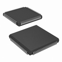
CY7C025-25AC Cypress Semiconductor Corp, CY7C025-25AC Datasheet - Page 5

CY7C025-25AC
Manufacturer Part Number
CY7C025-25AC
Description
IC,SRAM,8KX16,CMOS,QFP,100PIN,PLASTIC
Manufacturer
Cypress Semiconductor Corp
Datasheet
1.CY7C024-55AXC.pdf
(21 pages)
Specifications of CY7C025-25AC
Format - Memory
RAM
Memory Type
SRAM - Dual Port, Asynchronous
Memory Size
128K (8K x 16)
Speed
25ns
Interface
Parallel
Voltage - Supply
4.5 V ~ 5.5 V
Operating Temperature
0°C ~ 70°C
Package / Case
100-LQFP
Lead Free Status / RoHS Status
Contains lead / RoHS non-compliant
Available stocks
Company
Part Number
Manufacturer
Quantity
Price
Company:
Part Number:
CY7C025-25AC
Manufacturer:
CYPRESS
Quantity:
745
Company:
Part Number:
CY7C025-25AC
Manufacturer:
Cypress Semiconductor Corp
Quantity:
10 000
Semaphores are accessed by asserting SEM LOW. The SEM
pin functions as a chip select for the semaphore latches (CE
must remain HIGH during SEM LOW). A0–2 represents the
semaphore address. OE and R/W are used in the same manner
as a normal memory access. When writing or reading a
semaphore, the other address pins have no effect.
When writing to the semaphore, only I/O
written to the left port of an available semaphore, a one appears
at the same semaphore address on the right port. That
semaphore can now only be modified by the side showing zero
(the left port in this case). If the left port now relinquishes control
by writing a one to the semaphore, the semaphore is set to one
Table 1. Non-Contending Read/Write
Table 2. Interrupt Operation Example (Assumes BUSY
Document #: 38-06035 Rev. *D
Set Right INT
Reset Right INT
Set Left INT
Reset Left INT
CE
H
H
H
X
X
X
X
L
L
L
L
L
L
L
L
R/W
H
H
H
H
H
X
X
X
X
X
L
L
L
L
R
Flag
L
Flag
Function
R
Flag
Flag
OE
X
X
X
X
X
H
X
X
X
X
L
L
L
L
L
Inputs
UB
X
H
H
H
X
X
H
X
H
X
L
L
L
L
L
LB
X
H
H
H
X
X
H
X
H
X
L
L
L
L
L
0
R/W
is used. If a zero is
X
X
X
L
SEM
L
H
H
H
H
H
H
H
H
X
L
L
L
L
L
L
CE
X
X
L
L
L
High Z
High Z
High Z
Data In
Data In
High Z
Data Out
Data Out
High Z
Data Out
Data Out
Data In
Data In
I/O
Left Port
L
OE
=BUSY
X
X
X
L
0
–I/O
L
7
R
A
(1)FFE
[3]
(1)FFF
for both sides. However, if the right port had requested the
semaphore (written a zero) while the left port had control, the
right port immediately owns the semaphore as soon as the left
port released it.
When reading a semaphore, all sixteen/eighteen data lines
output the semaphore value. The read value is latched in an
output register to prevent the semaphore from changing state
during a write from the other port. If both ports attempt to access
the semaphore within t
definitely obtained by one side or the other, but there is no
guarantee which side controls the semaphore
=HIGH)
0L–11L
Outputs
X
X
High Z
High Z
Data In
High Z
Data In
Data Out
High Z
Data Out
High Z
Data Out
Data Out
Data In
Data In
[7]
I/O
INT
H
L
X
X
8
[8]
[9]
–I/O
L
Table 3
15
R/W
[4]
X
X
X
L
R
shows sample semaphore operations.
SPS
Deselected: Power Down
Deselected: Power Down
Write to Upper Byte Only
Write to Lower Byte Only
Write to Both Bytes
Read Upper Byte Only
Read Lower Byte Only
Read Both Bytes
Outputs Disabled
Read Data in Semaphore Flag
Read Data in Semaphore Flag
Write D
Write D
Not Allowed
Not Allowed
CE
X
X
L
L
R
of each other, the semaphore is
CY7C024/024A/0241
Right Port
IN0
IN0
OE
X
L
X
X
into Semaphore Flag
into Semaphore Flag
Operation
R
CY7C025/0251
A
(1)FFF
(1)FFE
0R–11R
X
X
Page 5 of 21
INT
H
L
X
X
[9]
[8]
R
[+] Feedback


