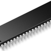
DSPIC33FJ16GS504-E/TL Microchip Technology, DSPIC33FJ16GS504-E/TL Datasheet - Page 5

DSPIC33FJ16GS504-E/TL
Manufacturer Part Number
DSPIC33FJ16GS504-E/TL
Description
16 Bit MCU/DSP 40MIPS 16 KB FLASH 2KB RAM SMPS 44 TLA 6x6x0.9 Mm TUBE
Manufacturer
Microchip Technology
Series
dsPIC™ 33Fr
Datasheet
1.DSPIC33FJ16GS404-ETL.pdf
(16 pages)
Specifications of DSPIC33FJ16GS504-E/TL
Core Processor
dsPIC
Core Size
16-Bit
Speed
40 MIPs
Connectivity
I²C, IrDA, LIN, SPI, UART/USART
Peripherals
Brown-out Detect/Reset, POR, PWM, WDT
Number Of I /o
35
Program Memory Size
16KB (16K x 8)
Program Memory Type
FLASH
Ram Size
2K x 8
Voltage - Supply (vcc/vdd)
3 V ~ 3.6 V
Data Converters
A/D 12x10b, D/A 1x10b
Oscillator Type
Internal
Operating Temperature
-40°C ~ 125°C
Package / Case
*
Processor Series
dsPIC33FJ
Core
dsPIC
Data Bus Width
16 bit
Data Ram Size
2 KB
Interface Type
I2C, SPI, UART
Maximum Clock Frequency
40 MHz
Number Of Programmable I/os
35
Operating Supply Voltage
3 V to 3.6 V
Maximum Operating Temperature
+ 125 C
Mounting Style
Through Hole
Development Tools By Supplier
DM240001, DM240002
Lead Free Status / RoHS Status
Lead free / RoHS Compliant
Eeprom Size
-
Lead Free Status / Rohs Status
Details
Power Supply Design Integration Levels
Level 3 Integration: Topology Control
This level permits the standard analog design to be reconfigured in addition to Level 1 and Level 2 features.
Changing the analog loop configuration and swapping between two different analog control loop filters can be
achieved. For example, a power supply can change from a PWM control loop to a hysteretic control loop at light
to the PWM modules in many ways through digital configuration. All pins associated with the error amplifiers and
comparators are available externally so any type of analog control loop can be created. Twelve ADC inputs are
available to monitor power supply operating parameters.
MCP1631HV Block Diagram
PIC16HV785 Boost LED Driver Application
OSC
Digital IO
SHDN
OSC
Up to
OV
16V
V
CS
FB
REF
DIS
IN
IN
Error Amp
Voltage
+
–
–
+
Over
OA1
UVLO
A1
1.2V
5V or 3.3V
Regulator
Shutdown
CPU
+
–
+
–
OA2
COMP2
+
–
PIC16HV785
C2
C1
+
–
Under Voltage
COMP1
Int OSC
Voltage
Ref.
V
BUS
10-bit ADC
5V Reg.
PWM
MCP1631HV
BOR
MCP1402
R
S
Q
G = +1
G = -10
1A Gate
Driver
A2
A3
(MCP9700A)
Temperature
Sensor
V
V
IS
IS
VS
VS
DD
EXT
IN
OUT
IN
OUT
LED
String
The MCP1631 high-speed PWM controller
can be used as a building block for
intelligent power supplies. The MCP1631
supplies the necessary analog peripherals,
including the error amplifier, comparator
and a high current output driver. The
voltage reference and switching clock are
supplied externally from an MCU. The MCU
can set the switching frequency of the
power stage, limit the maximum duty cycle
and adjust the phase of the switching clock
with respect to other power stages. The
rich feature set of the MCP1631 device
makes it a good fit for Level 2 and Level 3
intelligent power applications.
www.microchip.com/power
loads. This change would allow
a continuous inductor current
design to operate in discontinuous
conduction mode, increasing system
efficiency. Switching frequency
adjustment can also be used to
minimize losses. Microchip’s entire
range of MCUs and DSCs can assist
in Level 3 control applications. In
particular, mixed-signal solutions
such as the PIC16F785 integrate
an MCU with analog peripherals
and are well-suited for topology
control. In addition, the MCP1630
and MCP1631 PWM controllers are
designed for MCU power controller
applications.
The PIC16HV785 can be used in
a Level 3 application due to the
on-chip analog peripherals. The
device has two analog PWM modules
that can control power stages. Two
error amplifiers and two high-speed
comparators can be connected
5


