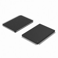
AD9860BST Analog Devices Inc, AD9860BST Datasheet - Page 20

AD9860BST
Manufacturer Part Number
AD9860BST
Description
IC FRONT-END MIXED-SGNL 128-LQFP
Manufacturer
Analog Devices Inc
Datasheet
1.AD9860BST.pdf
(32 pages)
Specifications of AD9860BST
Rohs Status
RoHS non-compliant
Rf Type
LMDS, MMDS
Features
10-bit ADCs, 12-bit DACs
Package / Case
128-LQFP
Operating Supply Voltage (max)
3.9V
Operating Temp Range
-40C to 70C
Operating Temperature Classification
Commercial
Package Type
LQFP
Mounting
Surface Mount
Pin Count
128
Lead Free Status / RoHS Status
Not Compliant
Available stocks
Company
Part Number
Manufacturer
Quantity
Price
Company:
Part Number:
AD9860BSTZ
Manufacturer:
ADI
Quantity:
285
AD9860/AD9862
The second interpolation filter will provide an additional 2 inter-
polation for an overall 4 interpolation. The second filter is a
15 tap filter. It suppresses out-of-band signals by 60 dB or more.
The flat passband response (less than 0.1 dB attenuation) is 38%
of the Tx input data rate (9.5% of f
data rate per channel is 32 MSPS per channel when using
4
The 2
shown in Figure 4a and 4b, respectively.
Fine Modulation Stage
A digital fine modulation stage is available in the transmit path to
shift the complex Tx output spectrum using a 24-bit numerically
controlled oscillator (NCO). To utilize the Fine Modulation
Block, 4
input date rate is 32 MSPS per channel, which generates a DAC
update rate, f
f
Modulation Stage precedes the Interpolation Filters, care must
be taken to ensure the entire desired signal is placed within the
pass band of the Interpolation Filter.
By default, the Fine Modulation Block is bypassed. To enable it
to perform a complex mix of the Tx I and Q data, Register 2’s data
paths, Fine Mod and Fine, should be configured. The NCO
frequency tuning word is set in the three FTW registers.
DAC
Figure 4. Spectral Response of 2
(top) and 4
interpolation.
, providing a step resolution of f
–100
–100
–10
–20
–30
–40
–50
–60
–70
–80
–90
–10
–20
–30
–40
–50
–60
–70
–80
–90
and 4
10
10
0
0
0
0
interpolation is required. Therefore, the maximum
DAC
0.1
0.1
Interpolation Filter (bottom)
, of 128 MSPS. The NCO can tune up to 1/4 of
Interpolation Filter Transfer function plots are
0.2
0.2
0.3
0.3
INCLUDUNG SIN (X)/X
NORMALIZED –
NORMALIZED –
0.4
0.4
INTERPOLATION
INCLUDUNG SIN (X)/X
0.5
0.5
INTERPOLATION
DAC
DAC
FILTER
FILTER
0.6
0.6
). The maximum input
f
f
/2
S
S
Interpolation Filter
26
0.7
0.7
. Since the Fine
0.8
0.8
0.9
0.9
1.0
1.0
–20–
Hilbert Filter
The Hilbert filter is available to provide a Hilbert transform of
“real” input data at a low intermediate frequency (IF) between
12.5% to 38% of the input data rate. The Hilbert filter essentially
transforms this “real,” single channel input data into a complex
representation (i.e., I and Q components) that can be used as
part of an image rejection architecture. The complex data can than
be processed further using the on-chip digital complex modulators.
The Hilbert filter requires 4 interpolation to be enabled and
accepts data at a maximum 32 MSPS. Figure 5 shows a spectral
plot of the Hilbert filter impulse response.
Latch/Demultiplexer
The AD9860/AD9862 Tx path accepts dual or single channel
data. The dual channel data can represent two independent real
signals or a complex signal. Various input data latching schemes
relative to one of the output clocks, CLKOUT1 or CLKOUT2,
are allowed, including using any combination of rising and falling
clock edges.
Associated Tx timing is discussed in detail in the Clock Overview
section of the data sheet.
TRANSMIT APPLICATIONS SECTION
The AD9860/AD9862 transmit path (Tx) includes two, high speed,
high performance, 12-/14-bit TxDACs. Figure 3 shows a detailed
block diagram of the transmit data path and can be referred to
throughout the explanation of the various modes of operation.
The various Tx modes of operation are broken into three parts,
determined by the format of the input data. They are:
1. Single Channel DAC Data
2. Two Independent Real Signal DAC Data (diversity or dual
3. Dual Channel Complex DAC Data (I and Q or Single Sideband)
Single Channel DAC Data
In this mode, 12-/14-bit single channel Tx data is provided to
the AD9860/AD9862 and latched using either CLKOUT1 or
CLKOUT2 edges as defined in the Clock Overview section of
the data sheet. All Tx digital signal processing blocks can be
utilized to address reconstruction filtering at the DAC output
and aid in frequency tuning.
channel
Figure 5. Tx Hilbert Filter, Keeping Positive
Frequencies Spectral Plot
–100
100
–20
–40
–60
–80
80
60
40
20
0
–20
–15
–10
FREQUENCY – MHz
–5
0
5
10
15
REV. 0
20


