MT9V131C12STC Aptina LLC, MT9V131C12STC Datasheet
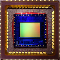
SENSOR IMAGE VGA COLOR 48CLCC

MT9V131C12STC

Manufacturer Part Number
MT9V131C12STC
Description
SENSOR IMAGE VGA COLOR 48CLCC
Manufacturer
Aptina LLC
Series
Micron®DigitalClarity®r
Type
CMOS Imagingr
Datasheet

Specifications of MT9V131C12STC

Package / Case
48-CLCC
Pixel Size
5.6µm x 5.6µm
Active Pixel Array
640H x 480V
Frames Per Second
15 ~ 90
Voltage - Supply
2.8V
Supply Voltage Range
2.55V To 3.05V
Operating Temperature Range
-20°C To +60°C
Digital Ic Case Style
CLCC
No. Of Pins
48
Supply Voltage Max
3.05V
Supply Voltage
RoHS Compliant
Ic Function
Digital Image Sensor
Rohs Compliant
Yes
Lead Free Status / RoHS Status
Lead free / RoHS Compliant
For Use With
557-1243 - KIT HEADBOARD FOR MT9V131557-1242 - KIT DEMO FOR MT9V131
Lead Free Status / RoHS Status
Lead free / RoHS Compliant
Other names
557-1241
1/4-Inch SOC VGA CMOS Digital Image
Sensor
MT9V131I29STC (iCSP)
MT9V131C12STC (CLCC)
Features
• Micron
• System-On-a-Chip (SOC)—Completely integrated
• Ultra low-power, high fidelity CMOS image sensor
• Superior low-light performance
• Up to 30 fps progressive scan at 27 MHz for high-
• On-chip image flow processor (IFP) performs
• Automatic exposure, white balance and black
• Xenon and LED-type flash support
• Two-wire serial programming interface
• Progressive scan ITU_R BT.656 (YCbCr), YUV,
Applications
• Security
• Biometrics
• Network cameras
• Toys and other battery-powered products
PDF: 09005aef824c99b3/Source: 009005aef824c99bb
MT9V131_LDS_1.fm - Rev. B 3/07 EN
‡Products and specifications discussed herein are for evaluation and reference purposes only and are subject to change by
camera system
quality video at VGA resolution
sophisticated processing: color recovery and
correction, sharpening, gamma, lens shading
correction, on-the-fly defect correction, 2X fixed
zoom
compensation, flicker avoidance, color saturation,
and defect identification and correction, auto frame
rate, back light compensation
565RGB, 555RGB, and 444RGB output data formats
Micron without notice. Products are only warranted by Micron to meet Micron’s production data sheet specifications.
®
DigitalClarity
®
CMOS imaging technology
MT9V131: 1/4-Inch SOC VGA CMOS Digital Image Sensor
1
Table 1:
The sensor is a complete camera-on-a-chip solution
and is designed specifically to meet the demands of
battery-powered products such as security cameras,
PDAs, and toys. It incorporates sophisticated camera
functions on-chip and is programmable through a
simple two-wire serial interface.
Ordering Information
Table 2:
MT9V131I29STC
MT9V131C12STC ES
MT9V131C12STCD ES Demo kit (color)
MT9V131C12STCH ES Demo kit headboard (color)
Optical format
Active imager size
Active pixels
Pixel size
Color filter array
Shutter type
Maximum data rate/
master clock
ADC resolution
Responsivity
Dynamic range
SNR
Supply voltage
Power consumption
Operating temperature
Packaging
Frame
rate
Part Number
MAX
Micron Technology, Inc., reserves the right to change products or specifications without notice.
Parameter
VGA (640 x 480)
CIF (352 x 288)
QVGA (320 x
240)
Key Performance Parameters
Available Part Numbers
44-Ball iCSP
48-Pin CLCC ES (color)
1/4-inch (4:3)
3.58mm(H) x 2.69mm(V)
4.48mm (diagonal)
640H x 480V (VGA)
5.6µm x 5.6µm
RGB Bayer pattern
Electronic rolling shutter (ERS)
12
24
15 fps at 12 MHz (default),
programmable up to 30 fps
at 27 MHz
Programmable up to 60 fps
Programmable up to 90 fps
10-bit, on-chip
1.9 V/lux-sec (550nm)
60dB
45dB
2.8V +0.25V
<80mW at 2.8V, 15 fps at 12MHz
44-Ball iCSP, 48-Pin CLCC
–20°C to +60°C
©2006 Micron Technology, Inc. All rights reserved.
13.5 Mp/s/
27 MHz
Description
Typical Value
Preliminary
Features

Related parts for MT9V131C12STC

MT9V131C12STC Summary of contents

Page 1

... Ordering Information Table 2: Available Part Numbers Part Number MT9V131I29STC MT9V131C12STC ES MT9V131C12STCD ES Demo kit (color) MT9V131C12STCH ES Demo kit headboard (color) Micron Technology, Inc., reserves the right to change products or specifications without notice. 1 ‡ Preliminary Features Typical Value 1/4-inch (4:3) 3 ...

Page 2

General Description This SOC VGA CMOS image sensor features DigitalClarity low-noise CMOS imaging technology that achieves CCD image quality (based on signal- to-noise ratio and low-light sensitivity) while maintaining the inherent size, cost, and integration advantages of CMOS. The MT9V131 ...

Page 3

Figure 1 illustrates the MT9V131 quantum efficiency in relation to wavelength. Figure 1: MT9V131 Quantum Efficiency vs. Wavelength Figure 2: Chip Block Diagram SCLK S DATA S ADDR CLK STANDBY OE# ...

Page 4

Figure 3 shows MT9V131 typical connections. For low-noise operation, the MT9V131 requires separate supplies for analog and digital power. Incoming digital and analog ground conductors can be tied together right next to the die. Both power supply rails should be ...

Page 5

Ball Assignment Figure 4: 44-Ball iCSP Pinout Diagram Figure 5: 48-Pin CLCC Pinout Diagram D OUT D OUT_ FLASH PIXCLK LINE_VALID FRAME_VALID PDF: 09005aef824c99b3/Source: 009005aef824c99bb MT9V131_LDS_2.fm - Rev. B 3/07 EN MT9V131: 1/4-Inch ...

Page 6

Table 4: Ball and Pin Description Symbol CLCC Pin CLKIN 20 SCLK ADDR ADC_TEST 31 RESET# 33 STANDBY 34 OE# 35 SCAN_EN DATA FLASH 13 PIXCLK 14 LINE_VALID 15 FRAME_VALID ...

Page 7

Image Flow Processor Overview of Architecture The image flow processor consists of a color processing pipeline and a measurement and control logic block, as shown in Figure 6 on page 8. The stream of raw data from the sensor enters ...

Page 8

Figure 6: Image Flow Processor Block Diagram The MT9V131 features smooth, continuous zoom and pan. This functionality is avail- able when the IFP output is downsized in the decimation block. The decimation block can downsize the original VGA image to ...

Page 9

Sensor Core Overview The sensor consists of a pixel array of 668 x 496 total, analog readout chain, 10-bit ADC with programmable gain and black offset, and timing and control. Figure 7: Sensor Core Block Diagram Sensor Array The sensor ...

Page 10

Electrical Specifications The recommended die operating temperature ranges from –20°C to +40°C. The sensor image quality may degrade above +40°C. Table 5: DC Electrical Characteristics 2.8 ± 0.25V Symbol Definition V Input high ...

Page 11

Table 6: AC Electrical Characteristics 2.8 ± 0.25V Definition Input clock frequency Clock duty cycle Input clock rise time Input clock fall time CLKIN to PIXCLK propagation LOW-to-HIGH delay HIGH-to-LOW PIXCLK to D ...

Page 12

Figure 9: 44-Ball iCSP Package Outline SEATING PLANE A 0.10 A 4.50 0.75 TYP BALL A7 44X Ø0.35 DIMENSIONS APPLY TO SOLDER BALLS POST REFLOW. THE PRE- REFLOW DIAMETER IS Ø0.33 4.50 0.75 TYP C L 2.25 7.00 ±0.075 SOLDER ...

Page 13

Figure 10: 48-Pin CLCC Package Outline D Seating plane A 8.8 0.8 47X 4.4 TYP 1.0 ±0 48X 0.40 ±0.05 8.8 4.4 4X 0.2 5.215 5.715 11.43 Lead finish: Au plating, 0.50 microns minimum thickness over Ni plating, ...

Page 14

Revision History Rev ...

Related keywords