25TTS08FPPBF Vishay, 25TTS08FPPBF Datasheet - Page 2
25TTS08FPPBF
Manufacturer Part Number
25TTS08FPPBF
Description
SCRs 800 Volt 25 Amp
Manufacturer
Vishay
Type
SCRr
Datasheet
1.25TTS12FPPBF.pdf
(7 pages)
Specifications of 25TTS08FPPBF
Breakover Current Ibo Max
350 A
Rated Repetitive Off-state Voltage Vdrm
800 V
Off-state Leakage Current @ Vdrm Idrm
0.5 mA
Forward Voltage Drop
1.25 V
Gate Trigger Voltage (vgt)
2 V
Maximum Gate Peak Inverse Voltage
10 V
Gate Trigger Current (igt)
45 mA
Holding Current (ih Max)
100 mA
Mounting Style
Through Hole
Package / Case
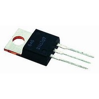
TO-220
Peak Repetitive Off-state Voltage, Vdrm
800V
Gate Trigger Current Max, Igt
45mA
Current It Av
16A
On State Rms Current It(rms)
25A
Peak Non Rep Surge Current Itsm 50hz
300A
Repetitive Peak Off-state Volt
800V
Off-state Voltage
800V
Average On-state Current
16A
Hold Current
100mA
Gate Trigger Current (max)
45mA
Gate Trigger Voltage (max)
2V
Peak Reverse Gate Voltage
10V
Package Type
TO-220 Full-Pak
Peak Repeat Off Current
500uA
Peak Surge On-state Current (max)
350A
On State Voltage(max)
1.25@16AV
Mounting
Through Hole
Pin Count
3 +Tab
Operating Temp Range
-40C to 125C
Operating Temperature Classification
Automotive
Lead Free Status / RoHS Status
Lead free / RoHS Compliant
Lead Free Status / RoHS Status
Lead free / RoHS Compliant, Lead free / RoHS Compliant
Available stocks
Company
Part Number
Manufacturer
Quantity
Price
Company:

Part Number:
25TTS08FPPBF
Manufacturer:
VIR
Quantity:
19 943


25TTS...FPPbF High Voltage Series
Vishay High Power Products
www.vishay.com
2
ABSOLUTE MAXIMUM RATINGS
PARAMETER
Maximum average on-state current
Maximum RMS on-state current
Maximum peak, one-cycle,
non-repetitive surge current
Maximum I
Maximum I
Maximum on-state voltage drop
On-state slope resistance
Threshold voltage
Maximum reverse and direct leakage current
Holding current
Maximum latching current
Maximum rate of rise of off-state voltage
Maximum rate of rise of turned-on current
TRIGGERING
PARAMETER
Maximum peak gate power
Maximum average gate power
Maximum peak positive gate current
Maximum peak negative gate voltage
Maximum required DC gate current to trigger
Maximum required DC gate
voltage to trigger
Maximum DC gate voltage not to trigger
Maximum DC gate current not to trigger
SWITCHING
PARAMETER
Typical turn-on time
Typical reverse recovery time
Typical turn-off time
2
2
t for fusing
√t for fusing
For technical questions, contact: diodes-tech@vishay.com
SYMBOL
SYMBOL
SYMBOL
TO-220AB FULL-PAK, 25 A
I
P
V
RM
- V
dV/dt
+ I
I
I
dI/dt
P
V
I
V
V
T(AV)
I
G(AV)
I
RMS
TSM
T(TO)
I
t
I
2
GT
GD
t
t
I
I
GM
2
TM
r
GT
GD
gt
/I
H
rr
q
√t
L
GM
GM
t
t
DM
Phase Control SCR
T
T
T
T
10 ms sine pulse, rated V
10 ms sine pulse, no voltage reapplied
10 ms sine pulse, rated V
10 ms sine pulse, no voltage reapplied
t = 0.1 to 10 ms, no voltage reapplied
16 A, T
T
T
Anode supply = 6 V, resistive load, initial I
Anode supply = 6 V, resistive load
Anode supply = 6 V, resistive load, T
Anode supply = 6 V, resistive load, T
Anode supply = 6 V, resistive load, T
Anode supply = 6 V, resistive load, T
Anode supply = 6 V, resistive load, T
Anode supply = 6 V, resistive load, T
T
J
J
J
C
J
J
J
= 125 °C
= 125 °C
= 25 °C
= 25 °C
= 125 °C
= 125 °C, V
= 85 °C, 180° conduction half sine wave
J
= 25 °C
DRM
V
TEST CONDITIONS
TEST CONDITIONS
TEST CONDITIONS
R
= Rated V
= Rated value
RRM
RRM
RRM
applied
applied
/V
DRM
J
J
J
J
J
J
= - 10 °C
= 25 °C
= 125 °C
= - 10 °C
= 25 °C
= 125 °C
T
= 1 A
Document Number: 94384
TYP. MAX.
VALUES
VALUES
VALUES
-
Revision: 27-May-08
6300
1.25
12.0
300
350
450
630
200
500
150
0.25
1.0
0.5
110
16
25
10
8.0
2.0
1.5
2.5
2.0
1.0
2.0
0.9
10
60
45
20
4
100
UNITS
UNITS
UNITS
A
V/µs
A/µs
A
mΩ
mA
mA
mA
µs
W
2
A
V
V
A
V
V
2
√s
s
Related parts for 25TTS08FPPBF
Image
Part Number
Description
Manufacturer
Datasheet
Request
R

Part Number:
Description:
SCR PHASE CONT 800V 25A TO-220AB
Manufacturer:
Vishay
Datasheet:

Part Number:
Description:
Phase Control SCR
Manufacturer:
International Rectifier Corp.
Datasheet:

Part Number:
Description:
357-036-542-201 CARDEDGE 36POS DL .156 BLK LOPRO
Manufacturer:
Vishay
Datasheet:
Part Number:
Description:
357-036-542-201 CARDEDGE 36POS DL .156 BLK LOPRO
Manufacturer:
Vishay
Datasheet:
Part Number:
Description:
357-036-542-201 CARDEDGE 36POS DL .156 BLK LOPRO
Manufacturer:
Vishay
Datasheet:
Part Number:
Description:
357-036-542-201 CARDEDGE 36POS DL .156 BLK LOPRO
Manufacturer:
Vishay
Datasheet:
Part Number:
Description:
357-036-542-201 CARDEDGE 36POS DL .156 BLK LOPRO
Manufacturer:
Vishay
Datasheet:
Part Number:
Description:
357-036-542-201 CARDEDGE 36POS DL .156 BLK LOPRO
Manufacturer:
Vishay
Datasheet:
Part Number:
Description:
357-036-542-201 CARDEDGE 36POS DL .156 BLK LOPRO
Manufacturer:
Vishay
Datasheet:
Part Number:
Description:
357-036-542-201 CARDEDGE 36POS DL .156 BLK LOPRO
Manufacturer:
Vishay
Datasheet:
Part Number:
Description:
357-036-542-201 CARDEDGE 36POS DL .156 BLK LOPRO
Manufacturer:
Vishay
Datasheet:
Part Number:
Description:
357-036-542-201 CARDEDGE 36POS DL .156 BLK LOPRO
Manufacturer:
Vishay
Datasheet:
Part Number:
Description:
357-036-542-201 CARDEDGE 36POS DL .156 BLK LOPRO
Manufacturer:
Vishay
Datasheet:
Part Number:
Description:
357-036-542-201 CARDEDGE 36POS DL .156 BLK LOPRO
Manufacturer:
Vishay
Datasheet:
Part Number:
Description:
357-036-542-201 CARDEDGE 36POS DL .156 BLK LOPRO
Manufacturer:
Vishay
Datasheet: