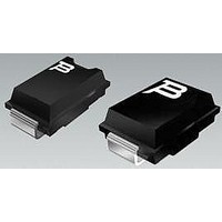
TISP4095J1BJR-S Bourns Inc., TISP4095J1BJR-S Datasheet - Page 9

TISP4095J1BJR-S
Manufacturer Part Number
TISP4095J1BJR-S
Description
Sidacs
Manufacturer
Bourns Inc.
Datasheet
1.TISP4080J1BJR-S.pdf
(12 pages)
Specifications of TISP4095J1BJR-S
Breakover Current Ibo Max
100 A
Rated Repetitive Off-state Voltage Vdrm
75 V
Off-state Leakage Current @ Vdrm Idrm
0.005 mA
Mounting Style
SMD/SMT
Package / Case
DO-214AA
Lead Free Status / RoHS Status
Lead free / RoHS Compliant
Available stocks
Company
Part Number
Manufacturer
Quantity
Price
Company:
Part Number:
TISP4095J1BJR-S
Manufacturer:
BOURNS
Quantity:
240 000
This protection configuration has three modes of protection. The RING to TIP terminal pair protection is given by the series combination of
protectors Th1a and Th1b, see Figure 11. The terminal pair protection voltage will be the sum of the V
V
protection voltage of ±400 V, Th1a and Th1b would have V
Similarly for the other terminal pairs, RING to GROUND protection is given by the series combination of Th1b and Th2 and the terminal pair
protection voltage is V
The maximum terminal pair voltage before clipping might occur is the sum of the protector V
TIP this will be 2 V
voltage of ±310 V. For RING to GROUND and TIP to GROUND terminal pairs, the maximum non-clipping signal voltage will be V
Under longitudinal surge conditions, when the prospective currents of the line conductors, I
protector, carries the sum of the Th1a and Th1b currents, see Figure 13. The current rating of Th2 must be twice that of Th1a and Th1b.
The main impulse waveforms of the standard are 500 A, 2/10 and 100 A, 10/1000. Assuming fuse current limiters, F1a and F1b, a suitable
Th1a and Th1b protector for these conductor currents is the TISP4xxxH3BJ series of devices. The ground return protector, Th2, must be rated
for at least 1000 A,2/10 and 200 A, 10/1000. A suitable Th2 protector for these ground currents is the TISP4xxxJ1BJ series of devices. This
arrangement is shown in Figure 14 and the following table lists all the catalogue device combinations.
Specifications are subject to change without notice.
Customers should verify actual device performance in their specific applications.
SEPTEMBER 2001 - REVISED JANUARY 2007
Y Configuration Design
GR-1089-CORE Designs
(BO)
RING
TIP
V
(BO)1
of Th1b. Protectors Th1a and Th1b are the same device type and the terminal pair protection voltage will be 2 V
Figure 11. Protection Voltage
RING to TIP Voltages
V
±116
±130
±150
±180
±200
±240
±270
±290
±310
±360
TISP4xxxJ1BJ Overvoltage Protector Series
DRM
V
+ V
(BO)2
V
(BO)1
V
Th1a
(BO)2
DRM1
2 V
(BO)1
. The ±200 V V
V
±140
±160
±190
±230
±250
±290
±330
±360
±400
±438
(BO)1
(BO)
V
+ V
Th1b
Th2
(BO)2
V
V
(BO)1
(BO)1
. TIP to GROUND protection voltage will also be V
(BO)1
+ V
AI4JAC
TIP to GROUND Voltages
(BO)2
V
±116
±130
±150
±180
±200
±240
±270
±290
±310
±360
protectors of the previous example have a V
DRM
V
RING to GROUND,
RING
TIP
V
APPLICATIONS INFORMATION
DRM1
Figure 12. Off-State Voltage
+ V
(BO)1
±140
±160
±190
±230
±250
±290
±330
±360
±400
±438
V
V
DRM2
DRM1
(BO)
= ±400/2 = ±200 V.
V
V
Th1a
DRM2
2 V
DRM1
I
Th1b
Th2
TISP4070H3BJ
TISP4080H3BJ
TISP4095H3BJ
TISP4115H3BJ
TISP4125H3BJ
TISP4145H3BJ
TISP4165H3BJ
TISP4180H3BJ
TISP4200H3BJ
TISP4219H3BJ
GR-1089-CORE Y Configuration Parts and Part Voltages
V
Th1a, Th1b
V
DRM1
DRM1
Part #
(BO)1
+ V
DRM
AI4JAB
+ V
DRM2
RING
of ±155 V, giving a maximum non-clipping signal
DRM
(BO)2
and I
, off-state voltages, see Figure 12. For RING to
.
RING
TIP
TIP
(BO)
TISP4070J1BJ
TISP4080J1BJ
TISP4095J1BJ
TISP4115J1BJ
TISP4125J1BJ
TISP4145J1BJ
TISP4165J1BJ
TISP4180J1BJ
TISP4200J1BJ
TISP4219J1BJ
, are equal, Th2, the ground return
Figure 13. Current Flow
, breakover voltage, of Th1a and the
Part #
Th1a
I
TIP
Th2
+
I
RING
I
TIP
(BO)1
. For a terminal pair
I
RING
Th2
V
±100
±120
±135
±145
±155
±180
±58
±65
±75
±90
DRM
V
DRM1
Th1b
+ V
±115
±125
±145
±165
±180
±200
±219
V
±70
±80
±95
AI4JAA
(BO)
V
DRM2
.


