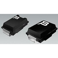
TISP4219J1BJR Bourns Inc., TISP4219J1BJR Datasheet - Page 11

TISP4219J1BJR
Manufacturer Part Number
TISP4219J1BJR
Description
Sidacs
Manufacturer
Bourns Inc.
Datasheet
1.TISP4080J1BJR-S.pdf
(12 pages)
Specifications of TISP4219J1BJR
Breakover Current Ibo Max
100 A
Rated Repetitive Off-state Voltage Vdrm
180 V
Off-state Leakage Current @ Vdrm Idrm
0.005 mA
Mounting Style
SMD/SMT
Package / Case
DO-214AA
Lead Free Status / RoHS Status
Lead free / RoHS Compliant
Available stocks
Company
Part Number
Manufacturer
Quantity
Price
Company:
Part Number:
TISP4219J1BJR-S
Manufacturer:
BOURNS
Quantity:
240 000
An ITU-T compliant design would probably require the replacement of the fuses by coordination resistors. With a ±410 V off-state voltage, this
may seem unnecessary as modern primary protectors will switch at lower voltages and automatically coordinate. On a perfect longitudinal
waveform this is true. However, the ITU-T also applies a transverse (metallic) test as well, to simulate non-simultaneous switching of the
primary protection. In this case, one conductor is grounded, which places the RING to TIP protection in parallel with the unswitched primary
protector. The ±270 V off-state voltage is likely to be lower than the primary switching voltage and there isn’t coordination. Under GR-1089-
CORE conditions with non-simultaneous switching, the 100 A 10/1000 current, which should have gone through the unswitched primary
protector, is diverted through the top arms of the Y into the switched primary, causing a 200 A current flow in that primary protector.
These designs are for special needs, where the RING to TIP protection voltage must be different to the RING to GROUND and TIP to
GROUND voltages. ADSL modem interfaces often have a need for asymmetric voltage limiting, see Figure 16. Here, the RING to TIP voltage
limitation is given by the d.c. blocking capacitor, C1, and the RING to GROUND and TIP to GROUND limitation is insulation breakdown. Often
the breakdown limit is set by the spacing of the PW (Printed Wiring) tracks. Figure 17 shows a solution. Using two ±165 V V
and Th1b, the RING to TIP voltage is limited to ±330 V. Using a higher voltage ±350 V V
Figure 17 and its following table is for a GR-1089-CORE compliant design.
Specifications are subject to change without notice.
Customers should verify actual device performance in their specific applications.
SEPTEMBER 2001 - REVISED JANUARY 2007
ITU-T K.20, K.45 and K.21 Designs (Continued)
Asymmetrical Designs
Figure 16. ADSL Modem Interface Voltage Limitations
RING to TIP Voltages
V
±270
RING to TIP Voltages
V
±550
±640
DRM
TISP4xxxJ1BJ Overvoltage Protector Series
V
DRM
V
RING
TIP
Voltage
V
±330
Limit
(BO)
V
C1
±700
±790
V
(BO)
V
Breakdown
Insulation
T1 or PW
TIP to GROUND Voltages
V
±410
C1
RING to GROUND,
DRM
V
TIP to GROUND Voltages
V
±550
±640
DRM
T1
V
RING to GROUND,
AI4JAH
±515
V
(BO)
V
±700
±790
V
(BO)
V
TISP4165H3BJ
Part #
Figure 17. Asymmetrical Design for US ADSL Modems
GR-1089-CORE Y Configuration Parts and Part Voltages
TISP3350T3BJ
TISP3395T3BJ
Th1a, Th1b
RING
Th1a + Th1b
TIP
Part #
ITU-T Y Configuration Parts and Part Voltages
(BO)
V
±135
F1b
F1a
DRM
V
part for Th2 limits the insulation stress to ±515 V.
TISP4165H3BJ
±165
Th1a
V
(BO)
V
R1a = R1b = 6.5 Ω
TISP4350J1BJ
TISP4395J1BJ
TISP4350J1BJ
Part #
Th2
Part #
TISP4350J1BJ
TISP4165H3BJ
Th2
Th1b
Th2
(BO)
V
±275
±320
DRM
parts for Th1a
±275
V
V
DRM
V
±350
±395
V
±350
V
(BO)
V
(BO)
V


