NCR169DRLRM ON Semiconductor, NCR169DRLRM Datasheet

SCRs 400V 800mA

NCR169DRLRM

Manufacturer Part Number
NCR169DRLRM
Description
SCRs 400V 800mA
Manufacturer
ON Semiconductor
Datasheet

Specifications of NCR169DRLRM

Breakover Current Ibo Max
10 A
Rated Repetitive Off-state Voltage Vdrm
400 V
Off-state Leakage Current @ Vdrm Idrm
0.01 mA
Forward Voltage Drop
1.7 V
Gate Trigger Voltage (vgt)
1.2 V
Maximum Gate Peak Inverse Voltage
5 V
Gate Trigger Current (igt)
0.2 mA
Holding Current (ih Max)
5 mA
Mounting Style
Through Hole
Package / Case
TO-92-3 (TO-226)
Lead Free Status / RoHS Status
Lead free / RoHS Compliant
Reverse Blocking Thyristor
applications such as relay and lamp drivers, small motor controls, gate
drivers for larger thyristors, and sensing and detection circuits.
Supplied in a cost effective plastic TO-226AA package.
1. V
This document contains information on a new product. Specifications and information
herein are subject to change without notice.
MAXIMUM RATINGS
December, 2000 – Rev. 0
Peak Repetitive Off–State Voltage (Note 1.)
On-State RMS Current
Peak Non-Repetitive Surge Current
Circuit Fusing Consideration (t = 10 ms)
Forward Peak Gate Power
Forward Average Gate Power
Forward Peak Gate Current
Reverse Peak Gate Voltage
Operating Junction Temperature Range
Storage Temperature Range
Other Logic Circuits
Sensitive Gate Allows Direct Triggering by Microcontrollers and
On–State Current Rating of 0.8 Amperes RMS at 80 C
Surge Current Capability – 10 Amperes
Immunity to dV/dt – 20 V/ sec Minimum at 110 C
Glass-Passivated Surface for Reliability and Uniformity
Device Marking: NCR169D, Date Code
Semiconductor Components Industries, LLC, 2000
apply for zero or negative gate voltage; however, positive gate voltage shall
not be applied concurrent with negative potential on the anode. Blocking
voltages shall not be tested with a constant current source such that the
voltage ratings of the devices are exceeded.
(T
60 Hz; Gate Open)
(T
(1/2 Cycle, Sine Wave, 60 Hz,
T
(T
(T
(T
(T
@ Rate V
DRM
PNPN device designed for line-powered general purpose
J
A
A
A
A
J
C
= 25 C)
= *40 to 110 C, Sine Wave, 50 to
= 25 C, Pulse Width v 1.0 s)
= 25 C, t = 20 ms)
= 25 C, Pulse Width v 1.0 s)
= 80 C) 180 Conduction Angles
and V
RRM
RRM
and V
Rating
for all types can be applied on a continuous basis. Ratings
DRM
(T
J
= 25 C unless otherwise noted)
Symbol
I
P
V
T(RMS)
V
V
I
P
G(AV)
I
T
DRM,
TSM
GRM
RRM
I
GM
T
GM
2
stg
J
t
–40 to
–40 to
Value
0.415
0.10
400
110
150
0.8
0.1
1.0
5.0
10
1
Amps
Volts
Volts
Amp
Watt
Watt
Amp
Unit
A
2
C
C
s
See detailed ordering and shipping information in the package
dimensions section on page 6 of this data sheet.
K
G
A
1
2
3
ORDERING INFORMATION
0.8 AMPERES RMS
A
http://onsemi.com
PIN ASSIGNMENT
Y
WW = Work Week
400 VOLTS
(TO–226AA)
CASE 029
STYLE 10
TO–92
= Year
SCR
Publication Order Number:
Cathode
Anode
Gate
G
MARKING
DIAGRAM
K
1 2 3
YWW
169D
NCR
NCR169D/D

Related parts for NCR169DRLRM

NCR169DRLRM Summary of contents

Page 1

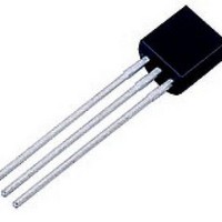
Reverse Blocking Thyristor PNPN device designed for line-powered general purpose applications such as relay and lamp drivers, small motor controls, gate drivers for larger thyristors, and sensing and detection circuits. Supplied in a cost effective plastic TO-226AA package. Sensitive Gate ...

Page 2

THERMAL CHARACTERISTICS Characteristic Thermal Resistance – Junction to Case – Junction to Ambient Lead Solder Temperature (t1/16 from case, 10 secs max) ELECTRICAL CHARACTERISTICS Characteristic OFF CHARACTERISTICS Peak Repetitive Forward or Reverse Blocking Current (Note 1 Rated V ...

Page 3

Voltage Current Characteristic of SCR Symbol Parameter V Peak Repetitive Off State Forward Voltage DRM I Peak Forward Blocking Current DRM V Peak Repetitive Off State Reverse Voltage RRM I Peak Reverse Blocking Current RRM V Peak on State Voltage ...

Page 4

T , JUNCTION TEMPERATURE ( C) J Figure 3. Typical Holding Current versus Junction Temperature 120 110 100 0.1 0.2 0.3 ...

Page 5

TO–92 EIA RADIAL TAPE IN FAN FOLD BOX OR ON REEL Symbol D Tape Feedhole Diameter D2 Component Lead Thickness Dimension F1, F2 Component Lead Pitch H Bottom of Component to Seating Plane H1 Feedhole Location H2A Deflection Left or ...

Page 6

... ORDERING & SHIPPING INFORMATION: MCR100 Series packaging options, Device Suffix Device NCR169D Bulk in Box (5K/Box) NCR169DRLRA Radial Tape and Reel (2K/Reel) NCR169DRLRM Radial Tape and Fan Fold Box (2K/Box) NCR169D Shipping Description of TO92 Tape Orientation N/A, Bulk Round side of TO92 and adhesive tape visible Flat side of TO92 and adhesive tape visible http://onsemi ...

Page 7

PACKAGE DIMENSIONS SECTION X– NCR169D TO–92 (TO–226AA) CASE 029–11 ISSUE http://onsemi.com 7 ...

Page 8

... Toll–Free from Mexico: Dial 01–800–288–2872 for Access – then Dial 866–297–9322 ASIA/PACIFIC: LDC for ON Semiconductor – Asia Support Phone: 303–675–2121 (Tue–Fri 9:00am to 1:00pm, Hong Kong Time) Toll Free from Hong Kong & Singapore: 001– ...

Page 9

WWW.ALLDATASHEET.COM Copyright © Each Manufacturing Company. All Datasheets cannot be modified without permission. This datasheet has been download from : www.AllDataSheet.com 100% Free DataSheet Search Site. Free Download. No Register. Fast Search System. www.AllDataSheet.com ...

Related keywords