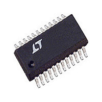
LTC4101EG#TR Linear Technology, LTC4101EG#TR Datasheet - Page 8

LTC4101EG#TR
Manufacturer Part Number
LTC4101EG#TR
Description
IC,Battery Management,CMOS,SSOP,24PIN,PLASTIC
Manufacturer
Linear Technology
Datasheet
1.LTC4101EGTR.pdf
(30 pages)
Specifications of LTC4101EG#TR
Output Voltage
5.504V
Operating Supply Voltage (min)
3V
Operating Supply Voltage (max)
5.5V
Operating Temp Range
-40C to 85C
Package Type
SSOP
Mounting
Surface Mount
Pin Count
24
Operating Temperature Classification
Industrial
Lead Free Status / Rohs Status
Not Compliant
Available stocks
Company
Part Number
Manufacturer
Quantity
Price
PIN FUNCTIONS
LTC4101
I
pin and GND. The value of the external resistor programs
the range and resolution of the programmed charger
current. This is a digital, not an analog, function.
V
this pin and GND. The value of the external resistor
programs the range and resolution of the charging
voltage. This is a digital, not an analog, function.
THB (Pin 15): SafetySignal Force/Sense Pin to Smart
Battery. See description of operation for more detail. The
maximum allowed combined capacitance on THA, THB and
SafetySignal is 1nF (see Figure 4). A series resistor 54.9k
needs to be connected between this pin and the battery’s
SafetySignal for this circuit to work correctly.
THA (Pin 16): SafetySignal Force/Sense Pin to Smart
Battery. See description of operation for more detail. The
maximum allowed combined capacitance on THA, THB
and SafetySignal is 1nF (see Figure 4). A series resistor
1130Ω needs to be connected between this pin and the
battery’s SafetySignal for this circuit to work correctly.
V
Circuitry. Bypass this pin with 0.1μF. Typically between
3.3V and 5V
V
Divider, which Provides Battery Voltage Feedback to the
Charger.
8
LIM
LIM
DD
SET
(Pin 13): An external resistor is connected between this
(Pin 17): Power Supply Input for the LTC4101 Digital
(Pin 14): An external resistor is connected between
(Pin 18): Tap Point of the Programmable Resistor
DC
.
I
Mode PWM. Higher I
current in normal operation. A 0.0015μF capacitor to GND
fi lters out PWM ripple. Typical full-scale output current is
40μA. Nominal voltage range for this pin is 0V to 3V.
I
CSP (Pin 21): Current Amplifi er CA1 Input. This pin
and the BAT pin measure the voltage across the sense
resistor, R
signals required for both peak and average current mode
operation.
BAT (Pin 22): Battery Sense Input and the Negative Refer-
ence for the Current Sense Resistor. A bypass capacitor
of at least 10μF is required.
CLN (Pin 23): Negative Input to the Input Current Limiting
Circuit Block. If no current limit function is desired, connect
this pin to CLP. The threshold is set at 100mV below the
voltage at the CLP pin. When used to limit supply current,
a fi lter is needed to fi lter out the switching noise.
CLP (Pin 24): Positive Input to the Input Current Limiting
Circuit Block. This pin also serves as a power supply for
the IC.
TH
DC
(Pin 19): Control Signal of the Inner Loop of the Current
(Pin 20): Bypass to GND with a 0.068μF Capacitor.
SENSE
, to provide the instantaneous current
TH
corresponds to higher charging
4101fa


