NJM2770R-TE1 NJR, NJM2770R-TE1 Datasheet

Audio Amplifiers High Pwr & Low V

NJM2770R-TE1

Manufacturer Part Number
NJM2770R-TE1
Description
Audio Amplifiers High Pwr & Low V
Manufacturer
NJR
Datasheet

Specifications of NJM2770R-TE1

Product
Class-AB
Output Power
400 mW
Thd Plus Noise
0.1 %
Operating Supply Voltage
3 V
Supply Current
2 mA
Maximum Power Dissipation
400 mW
Maximum Operating Temperature
+ 85 C
Mounting Style
SMD/SMT
Audio Load Resistance
16 Ohms
Input Bias Current (max)
0.1 uA
Input Signal Type
Differential
Minimum Operating Temperature
- 40 C
Output Signal Type
Differential
Supply Type
Single
Supply Voltage (max)
4.5 V
Supply Voltage (min)
2 V
Output Type
1-Channel Mono
Package / Case
VSP-8
Lead Free Status / RoHS Status
Lead free / RoHS Compliant
power amplifier with standby function. No external
coupling capacitors required because of the differential
output type. Two external resistors adjust the closed
loop gain. The output power is 250mW typical at
3V-supply 8ohm-load, and 400mW typical at 4.5v-supply
16ohm-load. The standby current is only 0.1 A typical.
PCS, codeless telephone, speaker amplifier for hands
free system, and especially cellular phone because of
low operating current, low standby current, and high
power output.
GENERAL DESCRIPTION
FEATURS
PIN CONFIGURATION & BLOCK DIAGRAM
The NJM2770 is high-power and low-voltage audio
The package of NJM2770 is VSP8, and suitable for
Operating Voltage
Operating Current
Low Power-Down Current
High Power Otput 250mW typ. at V
Gain Range at Voice Band
Load Impedance
Thermal Shut Down Function
Package Outline
Bipolar Technology
+V
HIGH-POWER & LOW-VOLTAGE AUDIO POWER AMPLIFIER
+V
-V
REF
IN
IN
4
3
2
400mW typ. V
145k
50k
50k
TSD
+2-+4.5V
2.0mA typ.,at V
0.1 A typ
Gv=0-43dB
R
VSP8,TVSP8
+
L
=4.5V,R
=4-200
GND
A
B
V
6
7
+
=3V,R
+
40k
40k
BIAS
L
L
=16
=8
+
=3V
5
8
1
V
CD
V
OUT
OUT
1
2
PACKAGE OUTLINE
Pin Function
1.CD
2.+V
3.+V
4.-V
5.V
6.V
7.GND
8.V
NJM2770R
OUT
OUT
+
IN
REF
IN
1
2
NJM2770
NJM2770RB1
- 1 -

Related parts for NJM2770R-TE1

NJM2770R-TE1 Summary of contents

Page 1

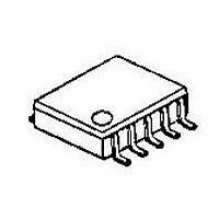
... REF 50k +2-+4.5V + 2.0mA typ.,at V =3V 0.1 A typ + =3V =4.5V,R =16 L Gv=0-43dB R =4-200 L VSP8,TVSP8 + V 6 BIAS OUT 40k 40k OUT TSD 7 GND NJM2770 PACKAGE OUTLINE NJM2770R NJM2770RB1 Pin Function 1.CD 2.+V REF 3.+V IN 4.-V IN 5.V 1 OUT + 6.V 7.GND 8.V 2 OUT - 1 - ...

Page 2

ABSOLUTE MAXIMUM RATINGS PARAMETER Supply Voltage Power Dissipation Operating Temperature Range Storage Temperature Range ELECTRICAL CHARACTERISTICS (V PARAMETER SYMBOL + Operating Voltage Range V Operating Current I CC Power Down Current I CCD Open Loop Gain Closed ...

Page 3

APPLICATION CURCUIT Ci Ri INPUT 0.1 F 20k 4.7 F note:1.The CD terminal(1pin) should connect High level( 2.0V), when NJM2770 is active. The standby mode, when the CD terminal is Low level( 0.8V). 2.To ...

Page 4

MEMO NJM2770 [CAUTION] The specifications on this databook are only given for information , without any guarantee as regards either mistakes or omissions. The application circuits in this databook are described only to show representative usages of the product and ...

Related keywords