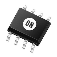
MC10EP33D ON Semiconductor, MC10EP33D Datasheet - Page 4

MC10EP33D
Manufacturer Part Number
MC10EP33D
Description
Clock Drivers & Distribution 3.3V/5V ECL Divide
Manufacturer
ON Semiconductor
Datasheet
1.MC10EP33D.pdf
(11 pages)
Specifications of MC10EP33D
Mounting Style
SMD/SMT
Package / Case
SOIC-8
Lead Free Status / RoHS Status
Lead free / RoHS Compliant
Available stocks
Company
Part Number
Manufacturer
Quantity
Price
Company:
Part Number:
MC10EP33DG
Manufacturer:
ON Semiconductor
Quantity:
135
Company:
Part Number:
MC10EP33DTG
Manufacturer:
ON Semiconductor
Quantity:
135
Part Number:
MC10EP33DTR2
Manufacturer:
ON/安森美
Quantity:
20 000
Part Number:
MC10EP33DTR2G
Manufacturer:
ON/安森美
Quantity:
20 000
NOTE: Device will meet the specifications after thermal equilibrium has been established when mounted in a test socket or printed circuit
6. Input and output parameters vary 1:1 with V
7. All loading with 50 W to V
8. V
NOTE: Device will meet the specifications after thermal equilibrium has been established when mounted in a test socket or printed circuit
9. Input and output parameters vary 1:1 with V
10. All loading with 50 W to V
11. V
Table 6. 10EP DC CHARACTERISTICS, PECL
Symbol
Table 7. 10EP DC CHARACTERISTICS, NECL
Symbol
I
V
V
V
V
V
V
I
I
I
VOH
V
V
V
V
V
I
I
EE
IH
IL
EE
IH
IL
OH
OL
IH
IL
BB
IHCMR
OL
IH
IL
BB
IHCMR
input signal.
input signal.
IHCMR
IHCMR
board with maintained transverse airflow greater than 500 lfpm. Electrical parameters are guaranteed only over the declared
operating temperature range. Functional operation of the device exceeding these conditions is not implied. Device specification limit
values are applied individually under normal operating conditions and not valid simultaneously.
min varies 1:1 with V
min varies 1:1 with V
Power Supply Current
Output HIGH Voltage (Note 7)
Output LOW Voltage (Note 7)
Input HIGH Voltage (Single−Ended)
Input LOW Voltage (Single−Ended)
Output Voltage Reference
Input HIGH Voltage Common Mode
Range (Differential Configuration) (Note 8)
Input HIGH Current
Input LOW Current
Power Supply Current
Output HIGH Voltage (Note 10)
Output LOW Voltage (Note 10)
Input HIGH Voltage (Single−Ended)
Input LOW Voltage (Single−Ended)
Output Voltage Reference
Input HIGH Voltage Common Mode
Range (Differential Configuration)
(Note 11)
Input HIGH Current
Input LOW Current
Characteristic
Characteristic
CC
CC
EE
EE
− 2.0 V.
− 2.0 V.
, V
, V
IHCMR
IHCMR
max varies 1:1 with V
max varies 1:1 with V
CC
CC
. V
.
EE
−1135
−1935
−1210
−1935
−1510
Min
V
0.5
can vary +2.0 V to −0.5 V.
V
18
CC
CC
V
3865
3065
3790
3065
3490
Min
http://onsemi.com
2.0
0.5
EE
18
= 5.0 V, V
= 0 V; V
+2.0
CC
−40°C
−1010
−1810
−1410
CC
Typ
26
−40°C
. The V
. The V
3990
3190
3590
Typ
26
EE
4
EE
= −5.5 V to −3.0 V (Note 9)
−1685
−1610
−1310
−885
−885
Max
IHCMR
150
IHCMR
= 0 V (Note 6)
0.0
40
3315
3390
3690
4115
4115
Max
150
5.0
40
range is referenced to the most positive side of the differential
range is referenced to the most positive side of the differential
−1070
−1870
−1870
−1445
−1145
Min
0.5
18
3930
3130
3855
3130
3555
Min
V
2.0
0.5
18
EE
+2.0
−1745
−1345
−945
25°C
Typ
26
25°C
4055
3255
3655
Typ
26
−1620
−1545
−1245
−820
−820
Max
150
0.0
4180
3380
4180
3455
3755
40
Max
150
5.0
40
−1010
−1810
−1085
−1810
−1385
Min
3990
3190
3915
3190
3615
0.5
18
Min
2.0
0.5
18
V
EE
+2.0
−1685
−1285
85°C
−885
85°C
3315
3715
Typ
4115
Typ
26
26
−1560
−1485
−1185
−760
−760
4240
3440
4240
3515
3815
Max
Max
150
150
0.0
5.0
40
40
Unit
Unit
mA
mV
mV
mV
mV
mV
mA
mV
mV
mV
mV
mV
mA
mA
mA
mA
V
V


