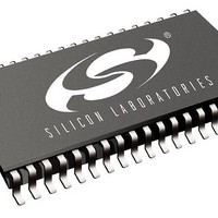
SI3210-BTR Silicon Laboratories Inc, SI3210-BTR Datasheet - Page 14

SI3210-BTR
Manufacturer Part Number
SI3210-BTR
Description
Telecom Line Management ICs Sgl Ch SLIC/Codec w/ DTMF Decoder
Manufacturer
Silicon Laboratories Inc
Datasheet
1.SI3210MPPQX-EVB.pdf
(146 pages)
Specifications of SI3210-BTR
Product
SLIC
Supply Voltage (min)
3.13 V
Supply Current
88 mA
Maximum Operating Temperature
+ 85 C
Minimum Operating Temperature
- 40 C
Mounting Style
SMD/SMT
Number Of Channels
1
Package / Case
TSSOP-38
Lead Free Status / RoHS Status
Lead free / RoHS Compliant
- Current page: 14 of 146
- Download datasheet (860Kb)
Table 11. Switching Characteristics—PCM Highway Serial Interface
V
Si3210/Si3211
14
PCLK Frequency
PCLK Duty Cycle Tolerance
PCLK-to-FSYNC Jitter Tolerance
Rise Time, PCLK
Fall Time, PCLK
Delay Time, PCLK Rise to DTX Active
Delay Time, PCLK Rise to DTX
Transition
Delay Time, PCLK Rise to DTX Tri-state
Setup Time, FSYNC to PCLK Fall
Hold Time, FSYNC to PCLK Fall
Setup Time, DRX to PCLK Fall
Hold Time, DRX to PCLK Fall
Notes:
D
= 3.13 to 5.25 V, T
1. All timing is referenced to the 50% level of the waveform. Input test levels are V
2. Not a valid PCLK frequency for GCI mode.
3. Specification applies to PCLK fall to DTX tri-state when that mode is selected (TRI = 0).
SCLK
SDO
Parameter
SDI
CS
A
= 0 to 70 °C for F-Grade, –40 to 85 °C for G-Grade, C
t
su1
t
d1
t
r
Figure 7. SPI Timing Diagram
3
Symbol
t
t
t
1/t
t
jitter
t
t
t
t
t
su1
su2
dty
t
d1
d2
d3
h1
h2
t
r
f
c
Rev. 1.5
t
su2
t
t
c
thru
Conditions
t
d2
t
Test
h2
L
= 20 pF
Min
–120
40
25
20
25
20
—
—
—
—
—
—
—
—
—
—
—
—
—
1
IH –
t
V
r
I/O –
t
h1
0.768
1.536
Typ
0.256
0.512
1.024
2.048
4.096
8.192
50
—
—
—
—
—
—
—
—
—
—
0.4V, V
1
2
2
t
cs
IL
t
d3
= 0.4 V.
Max
120
—
—
—
—
—
—
—
—
60
25
25
20
20
20
—
—
—
—
1
Units
MHz
MHz
MHz
MHz
MHz
MHz
MHz
MHz
ns
ns
ns
ns
ns
ns
ns
ns
ns
ns
%
Related parts for SI3210-BTR
Image
Part Number
Description
Manufacturer
Datasheet
Request
R
Part Number:
Description:
C°/SI3210 QFN EVALUATION BOARD WITH DISCRETE LINE INTERFACE
Manufacturer:
Silicon Laboratories Inc
Datasheet:
Part Number:
Description:
QFN 38/I°/SINGLE-CHANNEL SLIC/CODEC WITH DTMF DECODER AND BJT/INDUCTOR DC-D
Manufacturer:
Silicon Laboratories Inc
Part Number:
Description:
IC SLIC/CODEC PROGRAMMBL 38TSSOP
Manufacturer:
Silicon Laboratories Inc
Datasheet:
Part Number:
Description:
IC SLIC/CODEC PROG 38TSSOP
Manufacturer:
Silicon Laboratories Inc
Datasheet:

Part Number:
Description:
IC SLIC/CODEC PROG 38QFN
Manufacturer:
Silicon Laboratories Inc
Datasheet:
Part Number:
Description:
IC PROSLIC W/DC-DC CONV 38TSSOP
Manufacturer:
Silicon Laboratories Inc
Datasheet:
Part Number:
Description:
IC SLIC/CODEC PROG 38TSSOP
Manufacturer:
Silicon Laboratories Inc
Datasheet:

Part Number:
Description:
Telecom Line Management ICs Sgl Ch SLIC/Codec w/ DTMF Decoder
Manufacturer:
Silicon Laboratories Inc
Datasheet:
Part Number:
Description:
SLIC 1-CH 60dB 41mA 3.3V/5V 38-Pin QFN EP
Manufacturer:
Silicon Laboratories Inc
Datasheet:
Part Number:
Description:
Manufacturer:
Silicon Laboratories Inc
Datasheet:
Part Number:
Description:
Manufacturer:
Silicon Laboratories Inc
Datasheet:
Part Number:
Description:
SLIC 1-CH 60dB 41mA 3.3V/5V 38-Pin TSSOP T/R
Manufacturer:
Silicon Laboratories Inc
Datasheet:

Part Number:
Description:
SWITCH,DC-MAIN,ESTOP,32A
Manufacturer:
IMO PRECISION CONTROLS
Datasheet:

Part Number:
Description:
SWITCH,DISCONNECT,32A,DC
Manufacturer:
IMO PRECISION CONTROLS
Datasheet:
Part Number:
Description:
SMD/C°/SINGLE-ENDED OUTPUT SILICON OSCILLATOR
Manufacturer:
Silicon Laboratories Inc


