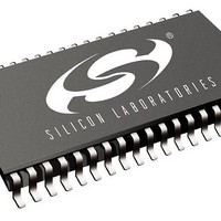
SI3210-BTR Silicon Laboratories Inc, SI3210-BTR Datasheet - Page 143

SI3210-BTR
Manufacturer Part Number
SI3210-BTR
Description
Telecom Line Management ICs Sgl Ch SLIC/Codec w/ DTMF Decoder
Manufacturer
Silicon Laboratories Inc
Datasheet
1.SI3210MPPQX-EVB.pdf
(146 pages)
Specifications of SI3210-BTR
Product
SLIC
Supply Voltage (min)
3.13 V
Supply Current
88 mA
Maximum Operating Temperature
+ 85 C
Minimum Operating Temperature
- 40 C
Mounting Style
SMD/SMT
Number Of Channels
1
Package / Case
TSSOP-38
Lead Free Status / RoHS Status
Lead free / RoHS Compliant
- Current page: 143 of 146
- Download datasheet (860Kb)
D
Revision 1.41 to Revision 1.42
Revision 1.42 to Revision 1.43
Revision 1.43 to Revision 1.44
OCUMENT
16-pin ESOIC dimension A1 corrected in Table 50
on page 135.
Delay time between chip selects, t
220 ns to 440 ns in Table 10 on page 13.
C10 changed from 22 nF to 0.1 µF in Figure 10 on
page 17.
C18, C19 changed from 1.0 µF to 4.7 µF in
Figure 12 on page 21.
Recommended value for Indirect Register 40
changed from 6 to 0 in Table 44 on page 123.
Added QFN package option.
Table 16, “Si3210/Si3210M External Component
Values—Discrete Solution,” on page 24.
"7. Ordering Guide" on page 129
Figure , “,” on page 16.
Figure 12, “Si3211 Typical Application Circuit Using
Si3201,” on page 21.
Figure 13, “Si3210/Si3210M Typical Application
Circuit Using Discrete Components,” on page 23.
Figure 14, “Si3211 Typical Application Circuit Using
Discrete Solution,” on page 25.
Table 52, “Package Diagram Dimensions,” on
page 137
Updated Figure 9.
Updated Figure 12.
Added TO-92 transistor suppliers to BOM.
Updated to include product revision designator.
“Lead-Free” changed to “Lead-Free and RoHS-
Compliant”
Added additional decoupling components to VDDA1,
VDDA2, and VDDD.
Added additional decoupling components to VDDA1,
VDDA2, and VDDD.
Added additional decoupling components to VDDA1,
VDDA2, and VDDD.
Added optional components to STIPE, SRINGE, and
SVBAT pins to improve idle channel noise.
Added additional decoupling components to VDDA1,
VDDA2, and VDDD.
Added optional components to STIPE, SRINGE, and
SVBAT pins to improve idle channel noise.
Changed A1 max dimension from 0.10 to 0.15.
Moved the schematic for the supply filtering network for
V
diagram to the top.
Moved the symbol for C26 closer to the V
the Si3201 symbol.
Changed R26 to 10 k.
Added Note 5.
DDA1
, V
DDA2
, and V
C
HANGE
DDD
from the bottom of the
L
IST
cs
, changed from
BATH
pin on
Rev. 1.5
Updated Figure 13.
Updated Figure 14.
Updated Table 3.
Updated Table 8.
Updated Table 11.
Updated Table 12.
Updated Table 13.
Updated Table 14.
Updated Table 15.
Moved the schematic for the supply filtering network for
V
diagram to the top.
Moved the symbol for C9 closer to the V
Si3201 symbol.
Changed R26 to 10 k.
Added Note 4.
Moved the schematic for the supply filtering network for
V
diagram to the top.
Added Note 5 and moved the symbol for C26 to better
illustrate its optimal position in a board layout.
Changed R26 to 10 k.
Added Note 6.
Moved the schematic for the supply filtering network for
V
diagram to the top.
Added Note 3 and moved the symbol for C26 to better
illustrate its optimal position in a board layout.
Added Note 4.
Changed R26 to 10 k.
Corrected connection between D1 and the linefeed
components.
Added Note 5
Corrected longitudinal current per pin for EBTO/
EBTA = 10 to 12 mA.
Filled-in typical values for I
V
Renamed "PCLK Period Jitter Tolerance" to
"PCLK-to-FSYNC Jitter Tolerance".
Added Note 2.
Changed current rating of L2 to 150 mA.
Added new row for R26 and changed the value to
10 k.
Added title for AN45 to description of R28 and R29.
Added column for component package type.
Added Note 1.
Added column for component package type.
Added column for component package type.
Changed current rating of L2 to 150 mA.
Added new row for R26 and changed the value to
10 k.
Rearranged the rows for R8 through R32 to be in
numerical order.
Added column for component package type.
Added Note 1.
DDA1
DDA1
DDA1
DDA
= 3.3 V.
, V
, V
, V
DDA2
DDA2
DDA2
, and V
, and V
, and V
Si3210/Si3211
DDD
DDD
DDD
from the bottom of the
from the bottom of the
from the bottom of the
VDD
and I
BAT
BATH
for V
DDD
pin on the
,
143
Related parts for SI3210-BTR
Image
Part Number
Description
Manufacturer
Datasheet
Request
R
Part Number:
Description:
C°/SI3210 QFN EVALUATION BOARD WITH DISCRETE LINE INTERFACE
Manufacturer:
Silicon Laboratories Inc
Datasheet:
Part Number:
Description:
QFN 38/I°/SINGLE-CHANNEL SLIC/CODEC WITH DTMF DECODER AND BJT/INDUCTOR DC-D
Manufacturer:
Silicon Laboratories Inc
Part Number:
Description:
IC SLIC/CODEC PROGRAMMBL 38TSSOP
Manufacturer:
Silicon Laboratories Inc
Datasheet:
Part Number:
Description:
IC SLIC/CODEC PROG 38TSSOP
Manufacturer:
Silicon Laboratories Inc
Datasheet:

Part Number:
Description:
IC SLIC/CODEC PROG 38QFN
Manufacturer:
Silicon Laboratories Inc
Datasheet:
Part Number:
Description:
IC PROSLIC W/DC-DC CONV 38TSSOP
Manufacturer:
Silicon Laboratories Inc
Datasheet:
Part Number:
Description:
IC SLIC/CODEC PROG 38TSSOP
Manufacturer:
Silicon Laboratories Inc
Datasheet:

Part Number:
Description:
Telecom Line Management ICs Sgl Ch SLIC/Codec w/ DTMF Decoder
Manufacturer:
Silicon Laboratories Inc
Datasheet:
Part Number:
Description:
SLIC 1-CH 60dB 41mA 3.3V/5V 38-Pin QFN EP
Manufacturer:
Silicon Laboratories Inc
Datasheet:
Part Number:
Description:
Manufacturer:
Silicon Laboratories Inc
Datasheet:
Part Number:
Description:
Manufacturer:
Silicon Laboratories Inc
Datasheet:
Part Number:
Description:
SLIC 1-CH 60dB 41mA 3.3V/5V 38-Pin TSSOP T/R
Manufacturer:
Silicon Laboratories Inc
Datasheet:

Part Number:
Description:
SWITCH,DC-MAIN,ESTOP,32A
Manufacturer:
IMO PRECISION CONTROLS
Datasheet:

Part Number:
Description:
SWITCH,DISCONNECT,32A,DC
Manufacturer:
IMO PRECISION CONTROLS
Datasheet:
Part Number:
Description:
SMD/C°/SINGLE-ENDED OUTPUT SILICON OSCILLATOR
Manufacturer:
Silicon Laboratories Inc


