IRFR320 Vishay, IRFR320 Datasheet - Page 2
IRFR320
Manufacturer Part Number
IRFR320
Description
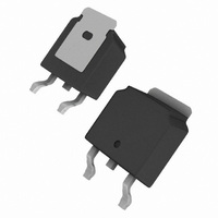
MOSFET N-CH 400V 3.1A DPAK
Manufacturer
Vishay
Datasheet
1.IRFR320.pdf
(8 pages)
Specifications of IRFR320
Fet Type
MOSFET N-Channel, Metal Oxide
Fet Feature
Standard
Rds On (max) @ Id, Vgs
1.8 Ohm @ 1.9A, 10V
Drain To Source Voltage (vdss)
400V
Current - Continuous Drain (id) @ 25° C
3.1A
Vgs(th) (max) @ Id
4V @ 250µA
Gate Charge (qg) @ Vgs
20nC @ 10V
Input Capacitance (ciss) @ Vds
350pF @ 25V
Power - Max
2.5W
Mounting Type
Surface Mount
Package / Case
DPak, TO-252 (2 leads+tab), SC-63
Lead Free Status / RoHS Status
Contains lead / RoHS non-compliant
Other names
*IRFR320
Available stocks
Company
Part Number
Manufacturer
Quantity
Price
Company:

Part Number:
IRFR320
Manufacturer:
IR
Quantity:
39 400
Company:
Part Number:
IRFR320A
Manufacturer:
IR
Quantity:
12 500
Company:
Part Number:
IRFR320M
Manufacturer:
IR
Quantity:
39 400
Company:
Part Number:
IRFR320PBF
Manufacturer:
IR
Quantity:
194
Part Number:
IRFR320TRPBF
Manufacturer:
VISHAY/威世
Quantity:
20 000
Company:
Part Number:
IRFR320TRRPBF
Manufacturer:
RENESAS
Quantity:
151
Part Number:
IRFR320TRRPBF
Manufacturer:
VISHAY/威世
Quantity:
20 000


IRFR320, IRFU320, SiHFR320, SiHFU320
Vishay Siliconix
Note
a. When mounted on 1" square PCB (FR-4 or G-10 material).
Notes
a. Repetitive rating; pulse width limited by maximum junction temperature (see fig. 11).
b. Pulse width ≤ 300 µs; duty cycle ≤ 2 %.
www.vishay.com
2
Maximum Junction-to-Ambient
Maximum Junction-to-Ambient
(PCB Mount)
THERMAL RESISTANCE RATINGS
PARAMETER
Maximum Junction-to-Case (Drain)
SPECIFICATIONS T
PARAMETER
Static
Drain-Source Breakdown Voltage
V
Gate-Source Threshold Voltage
Gate-Source Leakage
Zero Gate Voltage Drain Current
Drain-Source On-State Resistance
Forward Transconductance
Dynamic
Input Capacitance
Output Capacitance
Reverse Transfer Capacitance
Total Gate Charge
Gate-Source Charge
Gate-Drain Charge
Turn-On Delay Time
Rise Time
Turn-Off Delay Time
Fall Time
Internal Drain Inductance
Internal Source Inductance
Drain-Source Body Diode Characteristics
Continuous Source-Drain Diode Current
Pulsed Diode Forward Current
Body Diode Voltage
Body Diode Reverse Recovery Time
Body Diode Reverse Recovery Charge
Forward Turn-On Time
DS
Temperature Coefficient
a
J
a
= 25 °C, unless otherwise noted
SYMBOL
SYMBOL
ΔV
R
V
t
t
I
I
C
R
V
C
V
R
R
GS(th)
DS(on)
C
Q
Q
d(on)
d(off)
I
GSS
DSS
Q
g
Q
L
t
DS
L
SM
I
t
t
on
DS
oss
t
SD
thJA
thJA
thJC
iss
rss
S
rr
gd
fs
gs
r
f
D
S
g
rr
/T
J
Between lead,
6 mm (0.25") from
package and center of
die contact
MOSFET symbol
showing the
integral reverse
p - n junction diode
T
V
V
V
J
GS
GS
R
= 25 °C, I
DS
T
Intrinsic turn-on time is negligible (turn-on is dominated by L
G
J
Reference to 25 °C, I
= 10 V
= 10 V
= 25 °C, I
MIN.
= 320 V, V
= 18 Ω, R
V
-
-
-
V
V
V
V
f = 1.0 MHz, see fig. 5
DD
TEST CONDITIONS
DS
DS
GS
DS
= 400 V, V
= 200 V, I
F
= V
= 0 V, I
V
= 50 V, I
V
= 3.3 A, dI/dt = 100 A/µs
V
GS
DS
S
D
GS
I
GS
GS
D
= 3.1 A, V
= 56 Ω, see fig. 10
= ± 20 V
= - 25 V,
, I
= 3.3 A, V
= 0 V,
see fig. 6 and 13
= 0 V, T
D
D
D
= 250 µA
D
= 250 µA
I
GS
D
= 1.9 A
= 3.3 A,
= 1.9 A
D
TYP.
= 0 V
GS
= 1 mA
J
-
-
-
DS
= 125 °C
G
G
= 0 V
= 320 V,
b
D
S
b
b
b
D
S
b
MIN.
400
2.0
1.7
MAX.
-
-
-
-
-
-
-
-
-
-
-
-
-
-
-
-
-
-
-
-
-
-
110
3.0
50
S-82991-Rev. B, 12-Jan-09
Document Number: 91273
TYP.
0.51
350
120
270
4.5
7.5
1.4
47
10
14
30
13
-
-
-
-
-
-
-
-
-
-
-
-
-
± 100
MAX.
S
250
600
4.0
1.8
3.3
3.1
1.6
3.0
25
20
11
12
-
-
-
-
-
-
-
-
-
-
-
-
and L
UNIT
°C/W
D
UNIT
)
V/°C
nA
µA
nC
nH
µC
pF
ns
ns
V
V
Ω
S
A
V
Related parts for IRFR320
Image
Part Number
Description
Manufacturer
Datasheet
Request
R

Part Number:
Description:
357-036-542-201 CARDEDGE 36POS DL .156 BLK LOPRO
Manufacturer:
Vishay
Datasheet:
Part Number:
Description:
357-036-542-201 CARDEDGE 36POS DL .156 BLK LOPRO
Manufacturer:
Vishay
Datasheet:
Part Number:
Description:
357-036-542-201 CARDEDGE 36POS DL .156 BLK LOPRO
Manufacturer:
Vishay
Datasheet:
Part Number:
Description:
357-036-542-201 CARDEDGE 36POS DL .156 BLK LOPRO
Manufacturer:
Vishay
Datasheet:
Part Number:
Description:
357-036-542-201 CARDEDGE 36POS DL .156 BLK LOPRO
Manufacturer:
Vishay
Datasheet:
Part Number:
Description:
357-036-542-201 CARDEDGE 36POS DL .156 BLK LOPRO
Manufacturer:
Vishay
Datasheet:
Part Number:
Description:
357-036-542-201 CARDEDGE 36POS DL .156 BLK LOPRO
Manufacturer:
Vishay
Datasheet:
Part Number:
Description:
357-036-542-201 CARDEDGE 36POS DL .156 BLK LOPRO
Manufacturer:
Vishay
Datasheet:
Part Number:
Description:
357-036-542-201 CARDEDGE 36POS DL .156 BLK LOPRO
Manufacturer:
Vishay
Datasheet:
Part Number:
Description:
357-036-542-201 CARDEDGE 36POS DL .156 BLK LOPRO
Manufacturer:
Vishay
Datasheet:
Part Number:
Description:
357-036-542-201 CARDEDGE 36POS DL .156 BLK LOPRO
Manufacturer:
Vishay
Datasheet:
Part Number:
Description:
357-036-542-201 CARDEDGE 36POS DL .156 BLK LOPRO
Manufacturer:
Vishay
Datasheet:
Part Number:
Description:
357-036-542-201 CARDEDGE 36POS DL .156 BLK LOPRO
Manufacturer:
Vishay
Datasheet:
Part Number:
Description:
357-036-542-201 CARDEDGE 36POS DL .156 BLK LOPRO
Manufacturer:
Vishay
Datasheet:
Part Number:
Description:
357-036-542-201 CARDEDGE 36POS DL .156 BLK LOPRO
Manufacturer:
Vishay
Datasheet: