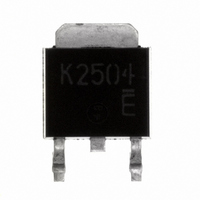
2SK2504TL Rohm Semiconductor, 2SK2504TL Datasheet - Page 4

2SK2504TL
Manufacturer Part Number
2SK2504TL
Description
MOSFET N-CH 100V 5A DPAK
Manufacturer
Rohm Semiconductor
Datasheet
1.2SK2504TL.pdf
(6 pages)
Specifications of 2SK2504TL
Fet Type
MOSFET N-Channel, Metal Oxide
Fet Feature
Logic Level Gate
Rds On (max) @ Id, Vgs
220 mOhm @ 2.5A, 10V
Drain To Source Voltage (vdss)
100V
Current - Continuous Drain (id) @ 25° C
5A
Vgs(th) (max) @ Id
2.5V @ 1mA
Input Capacitance (ciss) @ Vds
520pF @ 10V
Power - Max
20W
Mounting Type
Surface Mount
Package / Case
DPak, TO-252 (2 leads+tab), SC-63
Configuration
Single
Transistor Polarity
N-Channel
Resistance Drain-source Rds (on)
0.22 Ohm @ 4 V
Drain-source Breakdown Voltage
100 V
Gate-source Breakdown Voltage
+/- 20 V
Continuous Drain Current
5 A
Power Dissipation
20000 mW
Maximum Operating Temperature
+ 150 C
Mounting Style
SMD/SMT
Minimum Operating Temperature
- 55 C
Lead Free Status / RoHS Status
Lead free / RoHS Compliant
Gate Charge (qg) @ Vgs
-
Lead Free Status / Rohs Status
Lead free / RoHS Compliant
Other names
2SK2504TL
2SK2504TLTR
2SK2504TLTR
Transistors
Fig.15 Normalized Transient Thermal Resistance vs. Pulse Width
Fig.13
1000
0.05
500
200
100
0.5
0.2
0.1
50
20
10
10
0.05
5
2
5
2
1
0.001
0.01
0
10
0.1
Fig.10 Reverse Drain Current
1
10µ
V
Pulsed
0.2
D=1
0.5
0.1
0.05
SOURCE-DRAIN VOLTAGE : V
0.02
GS
0.1
Ta=125°C
(See Figures 16 and 17 for
resultant waveforms)
the measurement circuit and
=0V
Switching characteristics
DRAIN CURRENT : I
0.01
Single pulse
−25°C
vs. Source-Drain Voltage ( Ι )
0.2
75°C
25°C
100µ
0.5
0.5
PULSE WIDTH : PW
1m
1
t
t
t
d(off)
d(on)
t
r
f
1.0
2
D
(A)
Ta=25°C
V
V
R
Pulsed
DD
GS
G
10m
=10Ω
SD
=30V
=10V
5
(V)
(s)
1.5
10
Tc=25°C
θ
θ
100m
th(ch-c)
th(ch-c)
PW
=6.25°C/W
(t)=r (t) θ
0.05
0.01
1000
T
0.5
0.1
500
100
50
10
5
1
0.1
0
Fig.11 Reverse Drain Current
1
D= PW
Ta=25°C
di/dt=100A/µs
V
Pulsed
Fig.14 Reverse Recovery Time
GS
REVERSE DRAIN CURRENT : I
SOURCE-DRAIN VOLTAGE : V
T
th(ch-c)
=0V
0.2
V
vs. Source-Drain Voltage ( ΙΙ )
GS
vs. Reverse Drain Current
10
=10V
0.5
0.5
1
0V
1.0
2
T a =25°C
Pulsed
SD
DR
(V)
5
(A)
1.5
1
0
10000
1000
100
10
0.1
Fig.12 Typical Capacitance
DRAIN-SOURCE VOLTAGE : V
vs. Drain-Source Voltage
1
Rev.A
2SK2504
10
T a = 25°C
V
f = 1MHz
GS
DS
= 0V
(V)
4/5
100


