IRF2907ZSTRL7PP International Rectifier, IRF2907ZSTRL7PP Datasheet

MOSFET N-CH 75V 160A D2PAK-7

IRF2907ZSTRL7PP

Manufacturer Part Number
IRF2907ZSTRL7PP
Description
MOSFET N-CH 75V 160A D2PAK-7
Manufacturer
International Rectifier
Series
HEXFET®r
Datasheet

Specifications of IRF2907ZSTRL7PP

Fet Type
MOSFET N-Channel, Metal Oxide
Fet Feature
Standard
Rds On (max) @ Id, Vgs
3.8 mOhm @ 110A, 10V
Drain To Source Voltage (vdss)
75V
Current - Continuous Drain (id) @ 25° C
160A
Vgs(th) (max) @ Id
4V @ 250µA
Gate Charge (qg) @ Vgs
260nC @ 10V
Input Capacitance (ciss) @ Vds
7580pF @ 25V
Power - Max
300W
Mounting Type
Surface Mount
Package / Case
D²Pak, TO-263 (6 leads + tab)
Transistor Polarity
N Channel
Continuous Drain Current Id
180A
Drain Source Voltage Vds
75V
On Resistance Rds(on)
3mohm
Rds(on) Test Voltage Vgs
10V
Threshold Voltage Vgs Typ
4V
Lead Free Status / RoHS Status
Lead free / RoHS Compliant
Other names
IRF2907ZSTRL7PPTR
Features
l
l
l
l
l
HEXFET
Description
This HEXFET
processing techniques and advanced packaging
technology to achieve extremely low on-resistance
and world -class current ratings. Additional features
of this design are a 175°C junction operating tem-
perature, fast switching speed and improved repeti-
tive avalanche rating . These features combine to
make this design an extremely efficient and reliable
device for use in Server & Telecom OR'ing and low
voltage Motor Drive Applications.
Absolute Maximum Ratings
I
I
I
I
P
V
E
E
I
E
T
T
Thermal Resistance
R
R
R
R
www.irf.com
D
D
D
DM
AR
J
STG
D
GS
AS
AS
AR
JC
CS
JA
JA
@ T
@ T
@ T
@T
Advanced Process Technology
Ultra Low On-Resistance
175°C Operating Temperature
Fast Switching
Repetitive Avalanche Allowed up to Tjmax
(tested)
C
C
C
C
= 25°C
= 100°C
= 25°C
= 25°C
®
is a registered trademark of International Rectifier.
®
Power MOSFET utilizes the latest
Continuous Drain Current, V
Pulsed Drain Current
Maximum Power Dissipation
Linear Derating Factor
Gate-to-Source Voltage
Single Pulse Avalanche Energy (Thermally Limited)
Single Pulse Avalanche Energy Tested Value
Avalanche Current
Repetitive Avalanche Energy
Operating Junction and
Storage Temperature Range
Soldering Temperature, for 10 seconds
Mounting torque, 6-32 or M3 screw
Junction-to-Case
Case-to-Sink, Flat, Greased Surface
Junction-to-Ambient
Junction-to-Ambient (PCB Mount, steady state)
j
j
Parameter
Parameter
GS
GS
GS
g
@ 10V (Silicon Limited)
@ 10V (See Fig. 9)
@ 10V
(Package Limited)
IRF2907ZS-7PPbF
h
G
ij
d
300 (1.6mm from case )
HEXFET
See Fig.12a,12b,15,16
Typ.
S
D
0.50
–––
–––
–––
10 lbf•in (1.1N•m)
-55 to + 175
Max.
180
120
160
700
300
± 20
160
410
2.0
®
R
Power MOSFET
DS(on)
Max.
0.50
–––
V
62
40
I
DSS
D
= 160A
PD - 97031D
= 3.8m
= 75V
Units
Units
W/°C
°C/W
mJ
mJ
°C
W
A
V
A
1

Related parts for IRF2907ZSTRL7PP

IRF2907ZSTRL7PP Summary of contents

Page 1

... Mounting torque, 6- screw Thermal Resistance j R Junction-to-Case JC R Case-to-Sink, Flat, Greased Surface CS R Junction-to-Ambient JA R Junction-to-Ambient (PCB Mount, steady state) JA ® HEXFET is a registered trademark of International Rectifier. www.irf.com IRF2907ZS-7PPbF G Parameter @ 10V (Silicon Limited 10V (See Fig 10V (Package Limited Parameter 97031D ® ...

Page 2

Static @ T = 25°C (unless otherwise specified) J Parameter V Drain-to-Source Breakdown Voltage (BR)DSS Breakdown Voltage Temp. Coefficient DSS J R SMD Static Drain-to-Source On-Resistance DS(on) V Gate Threshold Voltage GS(th) gfs Forward Transconductance I Drain-to-Source ...

Page 3

PULSE WIDTH Tj = 25° Drain-to-Source Voltage (V) Fig 1. Typical Output Characteristics 1000 100 25° 175° ...

Page 4

0V MHZ C iss = SHORTED C rss = oss = 10000 C iss C oss 1000 ...

Page 5

Limited By Package 160 120 100 125 Case Temperature (°C) Fig 9. Maximum Drain Current vs. Case Temperature 0.50 0.20 0.1 0.10 0.05 0.02 0.01 0.01 SINGLE ...

Page 6

D.U 20V Fig 12a. Unclamped Inductive Test Circuit V (BR)DSS Fig 12b. Unclamped Inductive Waveforms Charge ...

Page 7

Duty Cycle = Single Pulse 100 0.01 0.05 10 0.10 1 1.0E-06 1.0E-05 Fig 15. Typical Avalanche Current vs.Pulsewidth 200 TOP Single Pulse BOTTOM 1% Duty Cycle 110A 150 100 100 ...

Page 8

D.U.T + ƒ ‚ -  SD Fig 17. Fig 18a. Switching Time Test Circuit V DS 90% 10 Fig 18b. Switching Time Waveforms 8 Driver Gate Drive P.W. D.U.T. I Waveform SD Reverse Recovery „ ...

Page 9

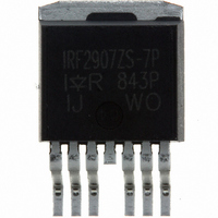
D Pak - 7 Pin Package Outline Dimensions are shown in millimeters (inches Pak - 7 Pin Part Marking Information Notes: 1. For an Automotive Qualified version of this part please see http://www.irf.com/product-info/auto/ 2. For the most ...

Page 10

D Pak - 7 Pin Tape and Reel IR WORLD HEADQUARTERS: 233 Kansas St., El Segundo, California 90245, USA Tel: (310) 252-7105 10 Data and specifications subject to change without notice. Visit us at www.irf.com for sales contact information. ...

Related keywords