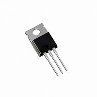
IRFB31N20DPBF International Rectifier, IRFB31N20DPBF Datasheet - Page 4

IRFB31N20DPBF
Manufacturer Part Number
IRFB31N20DPBF
Description
MOSFET N-CH 200V 31A TO-220AB
Manufacturer
International Rectifier
Series
HEXFET®r
Specifications of IRFB31N20DPBF
Fet Type
MOSFET N-Channel, Metal Oxide
Fet Feature
Standard
Rds On (max) @ Id, Vgs
82 mOhm @ 18A, 10V
Drain To Source Voltage (vdss)
200V
Current - Continuous Drain (id) @ 25° C
31A
Vgs(th) (max) @ Id
5.5V @ 250µA
Gate Charge (qg) @ Vgs
107nC @ 10V
Input Capacitance (ciss) @ Vds
2370pF @ 25V
Power - Max
3.1W
Mounting Type
Through Hole
Package / Case
TO-220-3 (Straight Leads)
Channel Type
N
Current, Drain
31 A
Gate Charge, Total
70 nC
Package Type
TO-220AB
Polarization
N-Channel
Power Dissipation
200 W
Resistance, Drain To Source On
0.082 Ohm
Resistance, Thermal, Junction To Case
0.75 °C/W
Temperature, Operating, Maximum
+175 °C
Temperature, Operating, Minimum
-55 °C
Time, Turn-off Delay
26 ns
Time, Turn-on Delay
16 ns
Transconductance, Forward
17 S
Voltage, Breakdown, Drain To Source
200 V
Voltage, Drain To Source
200 V
Voltage, Forward, Diode
1.3 V
Voltage, Gate To Source
±30 V
Transistor Polarity
N-Channel
Drain-source Breakdown Voltage
200 V
Gate-source Breakdown Voltage
30 V
Continuous Drain Current
31 A
Mounting Style
Through Hole
Gate Charge Qg
70 nC
Lead Free Status / RoHS Status
Lead free / RoHS Compliant
Other names
*IRFB31N20DPBF
Available stocks
Company
Part Number
Manufacturer
Quantity
Price
Part Number:
IRFB31N20DPBF
Manufacturer:
IR
Quantity:
20 000
IRFB/S/SL31N20DPbF
100000
10000
4
1000
100
1000
10
100
0.1
10
1
Fig 5. Typical Capacitance Vs.
Fig 7. Typical Source-Drain Diode
0.2
1
Drain-to-Source Voltage
V
V DS , Drain-to-Source Voltage (V)
SD
0.4
T = 175 C
Forward Voltage
J
,Source-to-Drain Voltage (V)
V GS = 0V,
C iss = C gs + C gd , C ds
C rss = C gd
C oss = C ds + C gd
10
0.6
°
Ciss
Crss
Coss
T = 25 C
0.8
J
f = 1 MHZ
100
°
V
1.0
GS
SHORTED
= 0 V
1.2
1000
1000
20
16
12
100
8
4
0
Fig 8. Maximum Safe Operating Area
10
0
1
I =
D
1
Fig 6. Typical Gate Charge Vs.
T
T
Single Pulse
C
J
18A
= 25 C
= 175 C
Gate-to-Source Voltage
OPERATION IN THIS AREA LIMITED
V
20
Q , Total Gate Charge (nC)
DS
°
G
°
, Drain-to-Source Voltage (V)
10
40
BY R
DS(on)
V
V
V
FOR TEST CIRCUIT
60
DS
DS
DS
SEE FIGURE
www.irf.com
100
= 160V
= 100V
= 40V
80
10us
100us
1ms
10ms
13
1000
100


