IXTK120N25P IXYS, IXTK120N25P Datasheet
Home Discrete Semiconductor Products MOSFETs, GaNFETs - Single IXTK120N25P
Manufacturer Part Number
IXTK120N25P
Description
MOSFET N-CH 250V 120A TO-264
Specifications of IXTK120N25P
Fet Type
MOSFET N-Channel, Metal Oxide
Fet Feature
Standard
Rds On (max) @ Id, Vgs
24 mOhm @ 500mA, 10V
Drain To Source Voltage (vdss)
250V
Current - Continuous Drain (id) @ 25° C
120A
Vgs(th) (max) @ Id
5V @ 500µA
Gate Charge (qg) @ Vgs
185nC @ 10V
Input Capacitance (ciss) @ Vds
8000pF @ 25V
Power - Max
700W
Mounting Type
Through Hole
Package / Case
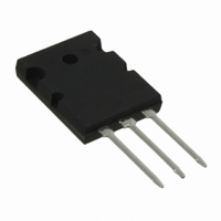
TO-264
Configuration
Single
Transistor Polarity
N-Channel
Resistance Drain-source Rds (on)
0.024 Ohms
Drain-source Breakdown Voltage
250 V
Gate-source Breakdown Voltage
+/- 20 V
Continuous Drain Current
120 A
Power Dissipation
700 W
Maximum Operating Temperature
+ 175 C
Mounting Style
Through Hole
Minimum Operating Temperature
- 55 C
Vdss, Max, (v)
250
Id(cont), Tc=25°c, (a)
120
Rds(on), Max, Tj=25°c, (?)
0.024
Ciss, Typ, (pf)
8700
Qg, Typ, (nc)
185
Trr, Typ, (ns)
200
Pd, (w)
700
Rthjc, Max, (k/w)
0.18
Package Style
TO-264
Lead Free Status / RoHS Status
Lead free / RoHS Compliant
Available stocks
PolarHT
Power MOSFET
N-Channel Enhancement Mode
Avalanche Rated
Symbol
V
V
V
V
I
I
I
I
E
E
dv/dt
P
T
T
T
T
T
M
Weight
Symbol
(T
BV
V
I
I
R
D25
D(RMS)
DM
AR
GSS
DSS
J
JM
stg
L
DSS
DGR
GS
GSM
AR
AS
D
SOLD
GS(th)
© 2006 IXYS All rights reserved
DS(on)
d
J
DSS
= 25° C, unless otherwise specified)
Test Conditions
T
T
Continuous
Transient
T
External lead current limit
T
T
T
T
I
T
T
1.6 mm (0.062 in.) from case for 10 s
Plastic body for 10 s
Mounting torque
Test Conditions
V
V
V
V
V
Pulse test, t ≤ 300 µs, duty cycle d ≤ 2 %
S
V
J
J
C
C
C
C
C
J
C
GS
DS
GS
DS
GS
GS
= 25° C to 175° C
= 25° C to 175° C; R
= 25° C
= 25° C, pulse width limited by T
= 25° C
= 25° C
= 25° C
≤ I
≤ 150° C, R
= 25° C
TM
= 0 V, I
= V
= ±20 V
= V
= 0 V
= 10 V, I
DM
, di/dt ≤ 100 A/µs, V
GS
DSS
, I
D
D
DC
D
= 250 µA
= 500µA
, V
G
= 0.5 I
= 4 Ω
DS
= 0
D25
GS
= 1 MΩ
DD
T
J
≤ V
= 125° C
IXTK 120N25P
DSS
JM
,
250
Min.
2.5
Characteristic Values
-55 ... +175
-55 ... +150
Maximum Ratings
Typ.
19
1.13/10 Nm/lb.in.
250
250
±20
±30
120
300
700
175
300
260
2.5
75
60
60
10
10
±200
250
Max.
5.0
25
24
V/ns
m Ω
mJ
° C
° C
nA
µA
µA
°C
°C
°C
W
V
V
V
V
A
A
A
A
V
V
g
J
TO-264 (IXTK)
Features
l
l
l
Advantages
l
l
l
International standard package
Unclamped Inductive Switching (UIS)
rated
Low package inductance
- easy to drive and to protect
Easy to mount
Space savings
High power density
G
D
G = Gate
S = Source
S
V
I
R
D25
DS(on)
DSS
= 250 V
= 120 A
≤ ≤ ≤ ≤ ≤ 24 m Ω Ω Ω Ω Ω
D = Drain
TAB = Drain
(TAB)
DS99175E(12/05)
Related parts for IXTK120N25P
IXTK120N25P Summary of contents
... GSS DSS DS DSS 0.5 I DS(on D25 Pulse test, t ≤ 300 µs, duty cycle d ≤ © 2006 IXYS All rights reserved IXTK 120N25P Maximum Ratings 250 = 1 MΩ 250 GS ±20 ±30 120 75 300 2.5 ≤ DSS 700 -55 ... +175 175 -55 ... +150 300 260 1 ...
... Pulse test, t ≤ 300 µs, duty cycle d ≤ -di/dt = 100 A/µ 100 IXYS reserves the right to change limits, test conditions, and dimensions. IXYS MOSFETs and IGBTs are covered by 4,835,592 one or moreof the following U.S. patents: 4,850,072 4,881,106 Characteristic Values (T = 25° C, unless otherwise specified) J Min. Typ. , pulse test 50 ...
... Volts D S Fig Norm alized to 0.5 I DS(on) Value vs. Drain Current 3.8 3.4 3 2.6 2.2 1 15V GS 1 120 150 I - Amperes D © 2006 IXYS All rights reserved C 250 225 200 175 150 125 100 2.5 3 3.5 C 2.8 9V 2.5 2.2 8V 1.9 7V 1.6 1.3 ...
... T = 150 0.2 0.4 0.6 0 olts S D Fig. 11. Capacitance 10000 1000 f = 1MH z 100 olts DS IXYS reserves the right to change limits, test conditions, and dimensions. 110 100 7 7.5 8 8.5 10 º 1.2 1.4 1.6 1000 100 C oss IXTK 120N25P Fig. 8. Trans conductance º ...
... © 2006 IXYS All rights reserved illis IXTK 120N25P ...
Related keywords
ixtk180n15 ixtk180n15p ixtk120n25p ixtk102n30p ixtk150n15p ixtk140n30p ixtk140n20p ixtk110n30 IXTK120N25P datasheet IXTK120N25P data sheet IXTK120N25P pdf datasheet IXTK120N25P component IXTK120N25P part IXTK120N25P distributor IXTK120N25P RoHS IXTK120N25P datasheet download