RJK03B9DPA-00#J53 Renesas Electronics America, RJK03B9DPA-00#J53 Datasheet
RJK03B9DPA-00#J53
Specifications of RJK03B9DPA-00#J53
Available stocks


Related parts for RJK03B9DPA-00#J53


RJK03B9DPA-00#J53 Summary of contents
Page 1
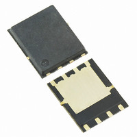
... RJK03B9DPA Silicon N Channel Power MOS FET Power Switching Features High speed switching Capable of 4.5 V gate drive Low drive current High density mounting Low on-resistance 8.3 m typ. ( DS(on) GS Pb-free Halogen-free Outline RENESAS Package code: PWSN0008DC-A ...
Page 2
... RJK03B9DPA Electrical Characteristics Item Drain to source breakdown voltage Gate to source leak current Zero gate voltage drain current Gate to source cutoff voltage Static drain to source on state resistance Forward transfer admittance Input capacitance Output capacitance Reverse transfer capacitance Gate Resistance Total gate charge ...
Page 3
... RJK03B9DPA Main Characteristics Power vs. Temperature Derating 100 Case Temperature Tc (°C) Typical Output Characteristics 20 4 3.0V 2 Drain to Source Voltage V Drain to Source Saturation Voltage vs. Gate to Source Voltage 400 300 200 100 Gate to Source Voltage V REJ03G1791-0320 Rev.3.20 May 12, 2010 1000 150 200 Pulse Test 2 ...
Page 4
... RJK03B9DPA Static Drain to Source On State Resistance vs. Temperature 20 Pulse Test 4 – Case Temperature Tc (°C) Dynamic Input Characteristics Gate Charge Qg (nc) Maximum Avalanche Energy vs. Channel Temperature Derating Channel Temperature Tch (°C) REJ03G1791-0320 Rev.3.20 May 12, 2010 10000 3000 1000 100 125 150 duty < 0.1% Rg ≥ ...
Page 5
... RJK03B9DPA Normalized Transient Thermal Impedance vs. Pulse Width 0.5 0.3 0.1 0.03 0.01 Avalanche Test Circuit V DS Monitor Rg Vin 15 V Switching Time Test Circuit Vin Monitor D.U.T. Rg Vin 10 V REJ03G1791-0320 Rev.3.20 May 12, 2010 θch – c(t) = γs (t) • θch – c θch – 5.0°C/ 25°C ...
Page 6
... Package Dimensions Package Name JEITA Package Code RENESAS Code ⎯ WPAK(2) PWSN0008DC-A 5.1 ± 0.2 1.27Typ 0.545Typ 4.90 ± 0.1 Ordering Information Part No. RJK03B9DPA-00-J53 3000 pcs REJ03G1791-0320 Rev.3.20 May 12, 2010 Previous Code MASS[Typ.] WPAK(2)V 0.07g 0.8Max 0.04Min 0.2Typ (Ni/Pd/Au plating) Quantity ...
Page 7
... Electronics product(s)" means any product developed or manufactured by or for Renesas Electronics. SALES OFFICES Refer to "http://www.renesas.com/" for the latest and detailed information. Renesas Electronics America Inc. 2880 Scott Boulevard Santa Clara, CA 95050-2554, U.S.A. Tel: +1-408-588-6000, Fax: +1-408-588-6130 Renesas Electronics Canada Limited ...