NTE4153NT1G ON Semiconductor, NTE4153NT1G Datasheet
NTE4153NT1G
Specifications of NTE4153NT1G
Available stocks


Related parts for NTE4153NT1G


NTE4153NT1G Summary of contents
Page 1
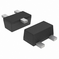
NTA4153N, NTE4153N Small Signal MOSFET 20 V, 915 mA, Single N−Channel with ESD Protection, SC−75 and SC−89 Features • Low R Improving System Efficiency DS(on) • Low Threshold Voltage, 1.5 V Rated • ESD Protected Gate • Pb−Free Packages are ...
Page 2
... Switching characteristics are independent of operating junction temperatures. ORDERING INFORMATION Device NTA4153NT1 NTA4153NT1G NTE4153NT1G †For information on tape and reel specifications, including part orientation and tape sizes, please refer to our Tape and Reel Packaging Specifications Brochure, BRD8011/D. NTA4153N, NTE4153N (T = 25°C unless otherwise stated) ...
Page 3
TYPICAL ELECTRICAL CHARACTERISTICS 1.2 2 0.8 0.6 0.4 0 0.5 1.0 1.5 2.0 2 DRAIN−TO−SOURCE VOLTAGE (VOLTS) DS Figure 1. On−Region Characteristics 0 4.5 ...
Page 4
TYPICAL ELECTRICAL CHARACTERISTICS 0.4 0.8 1 TOTAL GATE CHARGE (nC) G Figure 7. Gate−to−Source Voltage vs. Total Gate Charge 1 0.5 0.2 0.1 ...
Page 5
... L A1 SOLDERING FOOTPRINT* 1.803 0.071 0.508 0.020 *For additional information on our Pb−Free strategy and soldering details, please download the ON Semiconductor Soldering and Mounting Techniques Reference Manual, SOLDERRM/D. SC−75/SOT−416 CASE 463−01 ISSUE F NOTES: 1. DIMENSIONING AND TOLERANCING PER ANSI Y14.5M, 1982. ...
Page 6
... SCALE 10:1 details, please download the ON Semiconductor Soldering and Mounting Techniques Reference Manual, SOLDERRM/D. N. American Technical Support: 800−282−9855 Toll Free USA/Canada Europe, Middle East and Africa Technical Support: Phone: 421 33 790 2910 Japan Customer Focus Center Phone: 81− ...