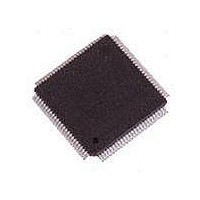
TDA8754HL17BE-T NXP Semiconductors, TDA8754HL17BE-T Datasheet - Page 15

TDA8754HL17BE-T
Manufacturer Part Number
TDA8754HL17BE-T
Description
Video ICs 3X8 BIT VIDEO A/D-170 MSPS
Manufacturer
NXP Semiconductors
Datasheet
1.TDA8754HL11C155.pdf
(57 pages)
Specifications of TDA8754HL17BE-T
Package / Case
SOT-486
Mounting Style
SMD/SMT
Lead Free Status / RoHS Status
Lead free / RoHS Compliant
Other names
TDA8754HL/17/C1,51
Philips Semiconductors
9397 750 14984
Product data sheet
8.2.4 Clamp
8.2.5 AGC
8.3 HSOSEL, DEO and SCHCKREFO
The reference ladders regulators are integrated.
Three independent parallel clamping circuits are used to clamp the video input signals on
programmable black levels. The clamp levels may be set from 24 to +136 LSBs in steps
of 1 LSB. They are controlled by three 9-bit I
OFFSETB).
The clamp pulse can be generated internally (based on the PLL clock reference) or can
be externally applied on pin CLP.
By setting correctly the I
Vsync signal. This inhibition will be effected by forcing logic 0 on the clamp request output.
It should be noted that the clamp period can start on the falling edge of the clamp request
and that the high level of the clamp request sets the ADC outputs in the blanking mode.
This means that by forcing the clamp signal request to logic 0 by using Vsync, a falling
edge may happen on the clamp request if this signal was at logic 1 before enforcing the
inhibition. To avoid this, the user has to guarantee that the Vsync signal used for the clamp
inhibition will not be set during a high level of the clamp request signal.
Remark: If signal Vsync is coming from the external pin VSYNC, this signal may be used
to coast the PLL. In order to properly do the coast, the edge of signal Vsync (COAST)
must not appear at the same time as the edge of signal Hsync. This condition is similar to
the pin CLP inhibition condition.
Three independent variable gain amplifiers are used to provide, for each channel, a
full-scale input signal to the 8-bit ADC. The gain adjustment range is designed in such a
way that for an input range varying from 0.5 to 1 V (p-p), the output signal corresponds to
the ADC full-scale input of 1 V (p-p).
Bit HSOSEL allows to have a full correlation phase behavior between outputs CKDATA
and HSYNCO when bit HSOSEL = 0 (Hsync from counter). If HSOSEL = 0 and bits PA4
to PA0 of register PHASE are changed to chose the best sampling time, the phase
relationship between outputs CKDATA and HSYNCO will stay unchanged. After the video
standard is determined, bit HSOSEL must be set to a logic 0 for normal operation mode.
To use the Hsync from the counter the registers HSYNCL, HBACKL, HDISPLMSB and
HDISPLLSB should be set properly in order to create the correct HSYNCO and DEO
output signals (see
signal DEO should be used to determine the first active pixel.
The demultiplexed mode should be used (bit DMX = 1) and the output flow is alternated
between port A and port B in case the sampling frequency is over 140 Msample/s (clock
frequency). It is necessary, in order to warrant that the outputs HSYNCO and DEO are
always changing on CKDATA output rising edge (see
HBACKL and HDISPL (see
outputs HSYNCO and DEO can change state during falling edge, which is not compliant
with the t
h(o)
and t
d(o)
Figure 5
specified output timing.
Rev. 06 — 16 June 2005
2
C-bus bits, it is possible to inhibit the clamp request with the
Figure
and
Figure
5) are even value. If an odd value is entered the
6), which is depending on video standard. Output
2
C-bus registers (OFFSETR, OFFSETG and
Triple 8-bit video ADC up to 270 Msps
Figure
© Koninklijke Philips Electronics N.V. 2005. All rights reserved.
7), that the values HSYNCL,
TDA8754
15 of 57


